Micron’s October 21 technology webinar laid out the most explicit 3D DRAM path the company has given the market. The plan extends 6F² through 1-delta in 2H 2027 and several more planar nodes, introduces wafer bonding at 1-epsilon, grows CMOS logic performance more than 10x by 2030, and skips the 4F² cell Samsung, SK hynix, and CXMT are pursuing. Scott DeBoer, President and Chief Technology and Products Officer, said AI-assisted engineering has cut Micron’s innovation-to-manufacturing time by 2x, the execution speed that determines when 3D DRAM ships. Futurum assesses the architecture call as correct and the 2027 schedule as the part still to be proven.
What Is Covered in This Article:
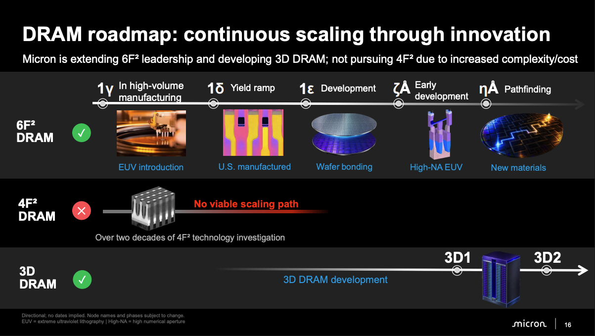
- A DRAM roadmap extending 6F² through 1-delta in 2H 2027 at a mid-20s percent density gain, wafer bonding at 1-epsilon, and zeta and eta nodes in pathfinding toward 3D DRAM
- Micron’s decision to skip 4F² as Samsung, SK hynix, and CXMT build it
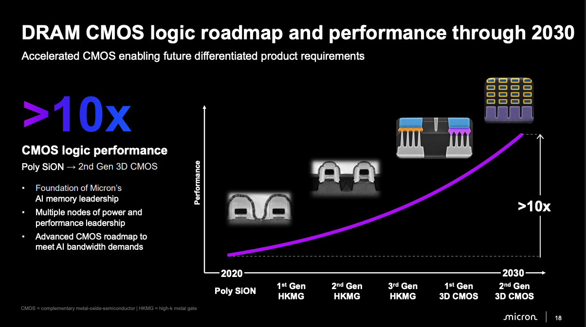
- A DRAM CMOS logic roadmap gaining more than 10x performance from 2020 to 2030 through 3D CMOS
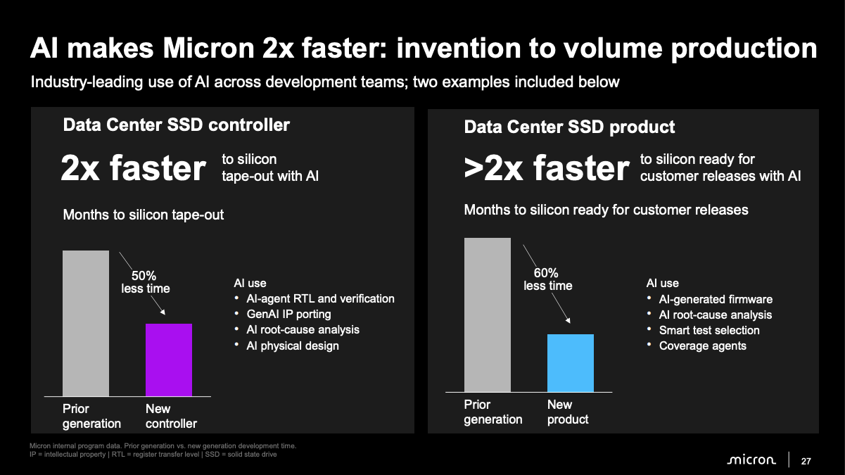
- AI-assisted engineering cutting innovation-to-manufacturing time by 2x
- HBM4 in high-volume manufacturing at 2.8 TB/s per stack and a vHBM and vEIM roadmap built on 1-delta
- DeBoer’s view that memory stays in short supply for at least the next two years
The News: Micron Technology hosted a technology webinar on October 21, 2026, with Scott DeBoer, President and Chief Technology and Products Officer, presenting the company’s DRAM, HBM, and NAND roadmaps and taking analyst questions. “We feel this is the strongest position Micron has ever been in terms of technology and product leadership,” said DeBoer in his opening remarks. The presentation disclosed the following roadmap items.
- The 1-gamma DRAM node and HBM4 are in high-volume manufacturing, with one HBM4 stack delivering 2.8 TB/s of bandwidth.
- The 1-delta node will ramp in 2H 2027 with a mid-20s percent bit density gain over 1-gamma, manufactured in the US, supporting HBM5, vHBM, and vEIM products.
- The 1-epsilon node will introduce wafer bonding, with zeta and eta nodes in pathfinding and 3D DRAM on the roadmap; Micron is extending 6F² and will not build 4F².
- DRAM CMOS logic performance improves more than 10x from 2020 to 2030, moving through three HKMG generations into 3D CMOS.
- LP6 targets over 35% better power than LP5, DDR6 targets over 2x DDR5 bandwidth, and a 512 GB DDR5 RDIMM at up to 9,200 MT/s has sampled with a 1 TB RDIMM shown as a capability.
- G11 NAND exceeds 400 layers, uses wafer-on-wafer bonding, roughly doubles G9 bit density, and ramps in 2H 2027.
- A token-efficiency roadmap runs from HBM4 through HBM6, vHBM 1 through 3, and vEIM 1 through 3, with vEIM 1 targeting 2 TB/s of bandwidth below 1 pJ/bit.
Micron Accelerates 3D DRAM From a Fifth Consecutive Node of Process Leadership
Analyst Take: Micron’s timely webinar displayed the practicality that built Micron’s current process lead. The company refuses to misdirect engineering resources where physics does not justify it. The 4F² skip applies that principle to the next decade. “DRAM is nearing atomic limits at this point, although we have confidence in several more planar nodes,” said DeBoer. The plan resolves that tension in the only direction the physics allows, building up, with 6F² extended through 1-delta, wafer bonding introduced at 1-epsilon, and 3D DRAM as the destination.
We find the architecture argument persuasive and the economics unproven, with three proofs standing between the roadmap and a modelable revenue line. Yield comes first, since bonded-wafer DRAM has no production history and the G11 wafer-on-wafer ramp in 2H 2027 is the nearest test of whether Micron’s bonding discipline transfers from a NAND string to a capacitor array. Cost per bit comes second. 3D DRAM adds wafer bonding and a reoriented cell, so it starts at a cost disadvantage and wins only once its per-layer gains undercut the shrinking per-node gains of the remaining planar roadmap, a crossover that took 3D NAND two to three generations to reach. The business model comes third, and it may debut with custom products, co-designed around customer base dies the way custom HBM already is, with fees and committed offtake announced before wafers move. A roadmap webinar is the venue for direction rather than commitments, so those gaps are expected. The direction deserves conviction yet the revenue opportunity is not yet easily modeled.
Skipping 4F² Routes All of Micron’s Scaling Capital Toward 3D
DeBoer dismantled the 4F² thesis in unusually direct terms, calling its claimed density benefit over 6F² “a bit of a myth” because capacitor pitch, in his telling, sets DRAM bit density, and summing up what ends planar scaling in two words, “it’s physics.” The field disagrees. Samsung has reportedly produced working 10A-class die using 4F² cells with vertical channel transistors and targets 2028 production, SK hynix sequences 4F² VG DRAM ahead of its own 3D transition, and TrendForce reports CXMT plans its first 4F² DRAM by the end of this year. Futurum sides with Micron on the physics, since 4F² shrinks the access transistor while the capacitor above it still sets the pitch. The process research mainstream agrees. Applied Materials’ DRAM Master Class framed capacitor patterning as the gating structure, and imec’s capacitorless IGZO DRAM program, published as a path to “disrupting the DRAM roadmap,” exists precisely because the capacitor is the constraint. The skip repeats the decision that produced Micron’s current lead of using DUV multipatterning through 1-alpha and 1-beta while rivals absorbed EUV’s early costs, then EUV at 1-gamma once it earned its place. The skip concentrates engineering, capital, and supplier co-development on a single architecture change, from planar 6F² directly to 3D DRAM, while rivals fund two, with wafer bonding arriving at 1-epsilon and G11’s 400-plus-layer wafer-on-wafer ramp as the proof that bonding works at production scale. If 4F² yields economically at 10A-class geometries, Micron has ceded a node of density. We assign that outcome low probability.
1-Delta Extends a Leadership Run That Began at 1z and Now Includes the Logic Under the Array
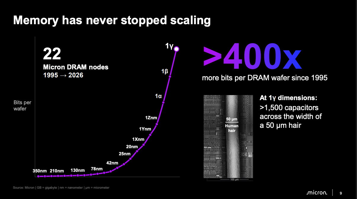
The webinar positioned process leadership as Micron’s enduring moat. The 1-delta node, ramping in 2H 2027 with a mid-20% bit density gain over 1-gamma and manufactured in the US, would be Micron’s fifth consecutive DRAM node brought to market first. The quieter disclosure sits under the array, where DRAM CMOS logic gains more than 10x performance from 2020 to 2030 on the way to 3D CMOS. That trajectory is what 3D DRAM, HBM base dies, and vEIM all draw on, and DeBoer confirmed in Q&A that HBM4E requires advanced base-die CMOS where HBM4 did not. In April, Futurum projected the data center off-chip memory market will grow from $96.8 billion in 2026 to $260.5 billion by 2030. The co-design slots decided over the next 18 months for the HBM4E and HBM5 generations are what convert leadership into share. Micron enters that window with the strongest hand it has had in the product’s history.
AI-Accelerated Execution Determines When 3D DRAM Arrives
DeBoer made the webinar’s sharpest commercial statement in Q&A, saying “we do not see a period of time where memory is not going to be in short supply in the next two years,” and declined to name a point where supply and demand balance. Futurum assesses that call as conservative. Asked by Daniel Newman of Futurum how Micron scales to meet compounding demand, DeBoer answered with execution speed, with AI-assisted engineering cutting innovation-to-manufacturing time by 2x, a data center SSD controller reaching tape-out in 50% less time, and a full SSD product customer-ready in 60% less time.
The research investments complete the picture Futurum sketched at Micron Research Labs’ announcement, where roughly $1 billion per year against Samsung’s approximately $25 billion in annual R&D closes the gap only by compounding through partners, visible here in High-NA EUV development with Albany NanoTech and supplier co-development in lithography, hybrid bonding enablement, and film processing. Applied Materials’ EPIC Center, opened this month with Micron as a founding partner, is the newest catalyst for that model, and DeBoer described its purpose in exactly those terms at the unveiling, co-investing in shared big bets to “make technology that maybe would have come out six years from now or seven years from now make it come out two years from now.” He also named the cross-ecosystem challenge that matters most to this roadmap, standardizing how 3D DRAM stacks on top of logic so the industry avoids one-off customized projects. The 2x claim is derived from SSD programs rather than DRAM nodes, and our skepticism concentrates on the 2H 2027 double ramp of 1-delta and G11.
What to Watch:
- Whether 1-delta ramps in 2H 2027 with the stated mid-20s percent density gain over 1-gamma
- Whether Micron commits to a 3D DRAM production window when 1-epsilon wafer bonding details emerge
- Whether Samsung’s 4F²-based 10A DRAM reaches its reported 2028 production target and enables a density comparison against 1-delta
- Whether CXMT ships its reported first 4F² DRAM by the end of 2026
- Whether G11 ships above 400 layers in 2H 2027 as the production proof of Micron’s wafer-bonding discipline
- Futurum’s AI Supply Chain Model forecast of DRAM and NAND supply tightness through 2030
Read the complete details on Micron Technology’s press release.
Sources
- Micron to Host Technology Webinar on Oct. 21, Micron, October 2026
- Micron to Host Technology Webinar on Oct. 21, Micron
Declaration of generative AI and AI-assisted technologies in the writing process: This content has been generated with the support of artificial intelligence technologies. Due to the fast pace of content creation and the continuous evolution of data and information, The Futurum Group and its analysts strive to ensure the accuracy and factual integrity of the information presented. However, the opinions and interpretations expressed in this content reflect those of the individual author/analyst. The Futurum Group makes no guarantees regarding the completeness, accuracy, or reliability of any information contained herein. Readers are encouraged to verify facts independently and consult relevant sources for further clarification.
Disclosure: Futurum is a research and advisory firm that engages or has engaged in research, analysis, and advisory services with many technology companies, including those mentioned in this article. The author does not hold any equity positions with any company mentioned in this article.
Analysis and opinions expressed herein are specific to the analyst individually and data and other information that might have been provided for validation, not those of Futurum as a whole.
Read the full Futurum Group Disclosure.
Other Insights From Futurum:
Micron Q4 FY 2026: AI Memory Demand Sustains Pricing Power
Micron Research Labs: Can $1 Billion a Year Out-Research Samsung and SK hynix?
Author Information

Brendan is Research Director, Semiconductors, Supply Chain, and Emerging Tech. He advises clients on strategic initiatives and leads the Futurum Semiconductors Practice. He is an experienced tech industry analyst who has guided tech leaders in identifying market opportunities spanning edge processors, generative AI applications, and hyperscale data centers.
Before joining Futurum, Brendan consulted with global AI leaders and served as a Senior Analyst in Emerging Technology Research at PitchBook. At PitchBook, he developed market intelligence tools for AI, highlighted by one of the industry’s most comprehensive AI semiconductor market landscapes encompassing both public and private companies. He has advised Fortune 100 tech giants, growth-stage innovators, global investors, and leading market research firms. Before PitchBook, he led research teams in tech investment banking and market research.
Brendan is based in Seattle, Washington. He has a Bachelor of Arts Degree from Amherst College.