Applied Materials introduced a suite of new DRAM and advanced packaging systems at its June 25 Master Class. The clearest signal was the migration of leading-edge logic process technology into memory, reaching from source/drain epitaxy to FinFET transistors to eBeam process control. That logic-class DRAM convergence could reshape where wafer fab equipment dollars flow as AI scales.
What Is Covered in This Article:
- Applied Materials introduced an enhanced Centura™ Prime™ Epi system that brings logic-class source/drain epitaxy to DRAM periphery transistors, paired with a 20% smaller footprint for higher tool density.
- New Opta™ Quad CMP, Nokota™ VMax™ 2 ECD, and Producer™ Avila™ 2 PECVD systems target the highest-value advanced packaging steps for HBM and 3D stacking.
- Two new eBeam systems, VeritySEM™ 7AP and SEMVision™ G7AP, carry wafer-fab metrology and defect review into advanced packaging.
- Applied framed a broad logic-memory convergence, as DRAM adopts epitaxy, FinFETs, and advanced wiring once reserved for leading-edge logic.
- Applied expects DRAM wafer fab equipment spending to double that of NAND in the medium-term, and advanced packaging revenue to grow more than 50% to over $2 billion in 2026.
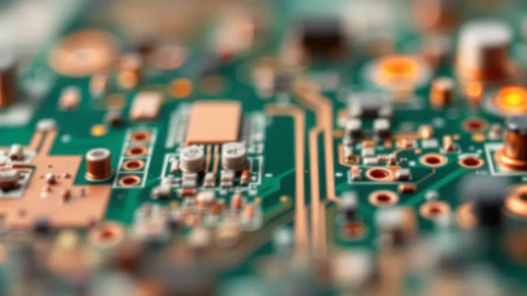
The News: On June 25, 2026, Applied Materials introduced a suite of new chipmaking systems for DRAM and advanced packaging, the two memory-side domains it argues will benefit most as AI compute scales. The launch spanned an enhanced Centura™ Prime™ Epi system for DRAM periphery transistors, three new systems for high-bandwidth memory (HBM) and 3D stacking, and two eBeam systems that bring wafer-fab-grade process control into packaging. Applied built the announcement around a single theme: as DRAM races to feed the bandwidth demands of AI, the process technology used to build memory has started to resemble leading-edge logic. The company shared the news at its DRAM and Advanced Packaging Master Class, the latest in a series that has tracked its push into the highest-value process inflections.
Applied Materials’ Master Class Schools Memory Makers on Logic-Class Fabrication
Analyst Take: Memory has become a strategic area of AI co-design. The memory wall, the widening gap between processor throughput and the rate at which DRAM can deliver data, has emerged as the binding constraint on AI performance. Dimensional scaling alone cannot close that gap. What can close it is materials scaling: porting the advanced epitaxy, transistor architectures, and metallization schemes that accelerated logic into the memory stack itself. That shift reframes DRAM not as a commodity companion to the processor, but as a co-designed performance layer whose speed, efficiency, and bandwidth are engineered in lockstep with the accelerator it feeds.
Applied Materials’ Master Class positioned material innovation ahead of new memory fabrication capacity that can come online as soon as 2028. The new Centura™ Prime™ Epi system grows doped silicon germanium in the source/drain regions of DRAM periphery transistors, the same logic-class epitaxy step that lifted drive current in leading-edge foundry nodes. FinFET transistors, advanced copper wiring, and wafer-fab-grade eBeam process control follow the same migration path. When the bottleneck is how fast memory can feed a processor, the process technology that built faster logic becomes the lever for faster memory, and memory makers become co-architects of AI system performance rather than capacity suppliers.
How Memory Fabrication Becomes More Like Logic
Applied has earned the right to make this argument. Back in 2013 its DRAM process equipment share sat below 15%. Roughly 10 points of share gain later, the company has reached the number one position, according to internal analysis. Three inflections drove that climb: capacitor patterning, the periphery transistor move to high-k metal gate, and HBM packaging. The new systems extend the same playbook. Logic-class DRAM now reaches across five inflections Applied laid out, from greater EUV use in 6F², to FinFET periphery transistors, to a CMOS-bonded array that builds memory and logic on separate wafers, to 4F² vertical cell transistors, and eventually to 3D DRAM. Each step pulls in tools where Applied already holds strong positions in epitaxy, etch, deposition, and process control.
The structural point is that every one of these DRAM scaling inflections is deposition and etch intensive. EUV patterning at 6F² demands more deposition and etch steps per layer. FinFET periphery transistors require epitaxial source/drain growth. CMOS-bonded arrays add wafer bonding, through-silicon vias, and additional deposition. 4F² vertical cell transistors extend the etch stack. Applied’s broad portfolio across epi, CVD, PVD, etch, CMP, plating, and process control positions it to capture wallet share at each inflection, rather than competing for a single step. The same logic applies on the packaging side, where taller HBM stacks, hybrid bonding, panel-level packaging, and co-packaged optics (CPO) each create incremental revenue streams across multiple tool types.
The financial framing reinforced the point. Applied expects DRAM wafer fab equipment spending to run well over twice NAND spending for the foreseeable future, a meaningful re-weighting from the earlier model that split memory evenly between the two. This view is consistent with Futurum’s forecast that DRAM revenue will increase from 2.0x NAND in 2025 to 2.4x by 2030. On the packaging side, the company expects advanced packaging revenue to grow more than 50% this year to over $2 billion, after the business more than tripled between 2020 and 2024. The AI-driven shift in wafer fab equipment mix toward leading-edge foundry-logic, DRAM, and advanced packaging aligns squarely with Applied’s strongest positions, and rising deposition and etch intensity in both DRAM and advanced packaging compounds the advantage.
Demand-side data supports the urgency. According to Futurum Group’s Semiconductors Decision Maker Survey, memory and storage availability ranks as the second-most-cited factor limiting AI cluster expansion, selected by 24% of respondents, behind only accelerator availability at 33%. That constraint gives memory makers and their equipment suppliers a structural tailwind as hyperscalers race to close the bandwidth gap.
Laser Focus on Advanced Packaging’s Process Control Problem
The DRAM thesis directly aligns with the expansion of the VeritySE and SEMVision eBeam systems into packaging with the 7AP and G7AP variants, respectively. eBeam process control uses a focused electron beam to measure nanometer-scale features and identify defects too small for optical tools. Similar to DRAM, packaging features have shrunk below the resolution limit of optical tools, and a single defect can scrap an entire HBM stack. Process control that once belonged to wafer fabs has therefore become a yield-defining requirement in packaging. With over 70% share in eBeam defect review, Applied is well-positioned to monetize that shift across silicon, organic, and glass substrates as the industry moves toward panel-level interposers and hybrid bonding. The optical process control market reached $13.8 billion in 2025. eBeam presents a similar market opportunity from a base of only $3.5 billion.
Stepping back, the through-line across DRAM, packaging, and process control was the same. The boundaries that defined memory, logic, and packaging as separate disciplines have blurred, and Applied has positioned its broad portfolio to sit at the seams. For investors and chipmakers tracking where the next wave of wafer fab equipment value will accrue, logic-class DRAM offers a useful lens. The companies that master the convergence on both the memory and process control sides will likely set the pace for AI chips through the rest of the decade.
The EPIC Center’s Platform for 3D DRAM Innovation
This pace of innovation positions the unveiled EPIC R&D Center as a strategic enabler of product launches. Applied has framed EPIC as a co-development hub where memory customers can prototype next-generation DRAM architectures, advanced packaging flows, and 3D integration schemes alongside Applied’s process engineers. For the inflections ahead, FinFET periphery, CMOS-bonded arrays, panel-level interposers, and eventually 3D DRAM, require tighter iteration loops between equipment maker and chipmaker than prior generations demanded. Memory customers that engage early in co-innovation at EPIC gain a development-time advantage over peers who wait for tools to reach volume readiness. For Applied, the center creates a pull-through dynamic where customers who co-develop on Applied platforms carry those process-of-record decisions into volume fabs. The newly opened Singapore advanced packaging facility extends the same logic into a region where HBM and advanced packaging capacity is expanding fastest. Together, the two facilities signal that Applied is investing not just in tools but in the ecosystem stickiness that turns a vendor relationship into a design-in advantage.
What to Watch:
- Migrating DRAM periphery transistors to FinFETs and adding epitaxy steps will raise process complexity and cost, and execution will likely vary across memory makers.
- HBM has carried much of the advanced packaging upside, so any mix shift to SRAM-based inference would test the durability of the greater-than-50% growth rate.
- Panel-level interposers in glass and laminate, along with hybrid bonding, remain early, and yield learning will set how quickly they scale.
- The EPIC Center and the Singapore advanced packaging facility will signal how aggressively customers plan to co-develop 3D DRAM and panel inflections. Early customer engagement at EPIC could accelerate process-of-record decisions and lock in Applied’s position ahead of volume ramps.
- Rising deposition and etch intensity across DRAM and advanced packaging inflections could compound Applied’s revenue opportunity at each node transition, making tool breadth a structural advantage over single-step competitors.
Read more about the new chipmaking systems on the Applied Materials website.
Sources
Declaration of generative AI and AI-assisted technologies in the writing process: This content has been generated with the support of artificial intelligence technologies. Due to the fast pace of content creation and the continuous evolution of data and information, The Futurum Group and its analysts strive to ensure the accuracy and factual integrity of the information presented. However, the opinions and interpretations expressed in this content reflect those of the individual author/analyst. The Futurum Group makes no guarantees regarding the completeness, accuracy, or reliability of any information contained herein. Readers are encouraged to verify facts independently and consult relevant sources for further clarification.
Disclosure: Futurum is a research and advisory firm that engages or has engaged in research, analysis, and advisory services with many technology companies, including those mentioned in this article. The author does not hold any equity positions with any company mentioned in this article.
Analysis and opinions expressed herein are specific to the analyst individually and data and other information that might have been provided for validation, not those of Futurum as a whole.
Read the full Futurum Group Disclosure.
Other Insights From Futurum:
Applied Materials’ EPIC Advanced Packaging Ecosystem Adds Broadcom to TSMC
Applied Materials Q2 FY 2026: AI Capacity Expansion Fuels Equipment Demand
Applied Materials and TSMC Partner to Drive Semiconductor R&D Roadmap
Author Information

Brendan is Research Director, Semiconductors, Supply Chain, and Emerging Tech. He advises clients on strategic initiatives and leads the Futurum Semiconductors Practice. He is an experienced tech industry analyst who has guided tech leaders in identifying market opportunities spanning edge processors, generative AI applications, and hyperscale data centers.
Before joining Futurum, Brendan consulted with global AI leaders and served as a Senior Analyst in Emerging Technology Research at PitchBook. At PitchBook, he developed market intelligence tools for AI, highlighted by one of the industry’s most comprehensive AI semiconductor market landscapes encompassing both public and private companies. He has advised Fortune 100 tech giants, growth-stage innovators, global investors, and leading market research firms. Before PitchBook, he led research teams in tech investment banking and market research.
Brendan is based in Seattle, Washington. He has a Bachelor of Arts Degree from Amherst College.