Micron named Deirdre Hanford corporate vice president and president of Micron Research Labs, the $10 billion long-horizon research institution announced in August 2026.
What Is Covered in This Article:
- Hanford’s appointment as corporate vice president and president of Micron Research Labs, reporting into Scott DeBoer’s Innovation, Technology and Products team
- Her background spanning 37 years at Synopsys, the founding CEO role at Natcast operating the NSTC, and recent advisory work across semiconductors, EDA, national defense, and AI
- The lab’s $10 billion planned budget over a decade, its Boise headquarters, and its research scope across memory process, architectures, packaging, and manufacturing
- Why an EDA leader running a memory lab points to design tools, base dies, and co-design as the next scaling frontier
The News: Micron Technology (Nasdaq: MU) announced on September 15 that Deirdre Hanford will lead Micron Research Labs as corporate vice president and president. She will establish the institution’s research infrastructure, operating model, and partnerships while defining a research agenda spanning Micron, academia, government, startups, and the wider industry ecosystem. She joins Scott DeBoer’s Innovation, Technology and Products leadership team.
Micron Research Labs, announced in August 2026, is headquartered in Boise, Idaho and backed by a planned $10 billion investment over the next decade. Micron positions it as the first dedicated memory research hub of its kind in the US, connected to the company’s research footprint across the US, Europe, Japan, India, Singapore, and Taiwan, with work spanning critical memory process technologies, future memory and compute architectures, advanced packaging, and next-generation semiconductor manufacturing. The lab sits on top of Micron’s separately announced US investment plan of more than $250 billion in manufacturing and R&D.
“Micron Research Labs was created to pursue the breakthroughs that will define the future of memory, compute and AI, and Deirdre is uniquely qualified to lead that mission,” said Scott DeBoer, President and Chief Technology and Products Officer of Micron Technology.
Hanford spent 37 years at Synopsys, where her roles included chief security officer, co-general manager of the Design Group, and executive vice president of customer engagement. She served as founding CEO of Natcast, the nonprofit operator of the CHIPS Act’s National Semiconductor Technology Center, and per Micron most recently advised leading organizations across semiconductors, electronic design automation, national defense, and AI. She sits on the UC Berkeley College of Engineering Advisory Board, the MIT School of Engineering Dean’s Advisory Council, and the SEMI Board of Industry Leaders, and received the 2025 IEEE Frederik Philips Award.
Micron Hires a 37-Year EDA Veteran to Run Its $10 Billion Memory Lab. What Does That Say About Where Memory Scaling Goes Next?
Analyst Take: Micron did not hire a DRAM process technologist to run its flagship research institution. It hired the executive who helped build the EDA industry’s market leader, then stood up the national research center created by the CHIPS Act. Futurum reads the choice as a statement about where memory differentiation now lives: in design, architecture, and ecosystem orchestration as much as in the fab. When Futurum assessed the lab’s August launch, the structure of the announcement was the story, since $1 billion a year cannot outspend Samsung’s roughly $25 billion annual R&D budget and must instead convene partners. Hanford is a convening hire. Her appointment moves the lab from launch toward execution and tells the industry which kind of breakthroughs Micron expects to matter.
Memory Scaling Has Become a Design Problem, and That Pulls It Into EDA’s Toolchain
The memory wall is no longer a lithography problem alone. Micron’s own Hot Chips 2026 presentation charted accelerator TFLOPS compounding at 3x every 2 years against HBM bandwidth compounding at under 2x, and its roadmap slide listed GPU offloading, advanced die-to-die PHYs, and custom features as the inflections ahead. Every one of those items is a logic design task. Custom HBM base dies built on logic processes require full digital implementation flows, IP integration, and verification; Samsung has said its HBM4 base dies already use a 4nm logic process. Multi-die packaging demands 3DIC co-design tools. Processing-in-memory places compute synthesis inside the DRAM vendor’s engineering scope for the first time. The suppliers that win the custom base-die era will look less like commodity DRAM makers and more like design houses with fabs attached.
Hanford ran customer engagement and co-managed the Design Group at the company whose tools every one of those flows depends on. The implication is that Micron wants its long-horizon research agenda set by someone fluent in the design-side transformation of memory rather than in bit-cost reduction, which the product organization already owns. Hanford’s Synopsys tenure also brings direct relationships with the accelerator designers, foundries, and IP vendors that a base die and co-design agenda has to recruit as partners. SK hynix characterized Micron’s HBM differentiation at Hot Chips as circuit design improvement plus an enhanced base die worth more than 20% energy efficiency gains, a rival’s framing that this appointment does nothing to contradict.
Frontier AI Labs Are Becoming Memory’s Most Demanding Design Partners
Micron’s release states that Hanford most recently advised leading organizations across semiconductors, EDA, national defense, and AI, and her advisory work included OpenAI. That connection matters more than a bio line. Frontier model developers have moved from buying whatever HBM ships to shaping silicon directly. OpenAI is co-developing custom accelerators with Broadcom, and every custom XPU program Futurum has tracked this year, from Marvell-Google to the NVIDIA-MediaTek NVLink Fusion alliance, treats the memory subsystem as a first-order design decision rather than a procurement line item. Decode-heavy agentic workloads price bandwidth per watt as the constraint on interactivity, which is a co-design problem between the model architecture, the accelerator, and the DRAM stack.
A research lab president who has advised a frontier lab arrives knowing the demand signal from the buyer that will define memory requirements five years out. The question her network raises is whether Micron Research Labs will treat frontier AI developers as research collaborators with seats at the agenda-setting table, the way IBM Research once treated its largest systems customers. An early named collaboration would confirm that possibility.
The Appointment Tests Whether Convening Power Substitutes for Spending Power
The bear case from Futurum’s August coverage still stands. Annual funding near $1 billion is below what Micron spends on R&D in a single quarter, and the lab’s flagship campus does not break ground until calendar 2027. Hanford has built a public-private research institution from zero in Natcast, and she also knows how slowly consortium research moves relative to a competitor’s in-house program. Samsung shipped LPDDR5X-PIM first. SK hynix is qualifying 16-high HBM4 stacks. A convening model produces papers and partnerships years before it produces process advantage, and Micron’s rivals are not waiting.
What to Watch:
- Whether the lab’s first named research partnerships include a frontier AI developer alongside the university and government collaborations already announced
- Whether senior technical hires under Hanford skew toward memory process and materials scientists or toward design and architecture leaders
- Whether the Boise flagship campus breaks ground on the calendar 2027 schedule
- Whether Micron discloses a base-die logic process node and foundry partner, the item its Hot Chips 2026 presentation left open
- Whether the lab’s charter comes to include custom DRAM dies for accelerator vendors, the category d-Matrix’s Raptor work has opened
Read more details about the announcement on Micron’s website.
Sources
- Micron Appoints Deirdre Hanford to Lead Micron Research Labs, Micron, September 2026
Declaration of generative AI and AI-assisted technologies in the writing process: This content has been generated with the support of artificial intelligence technologies. Due to the fast pace of content creation and the continuous evolution of data and information, The Futurum Group and its analysts strive to ensure the accuracy and factual integrity of the information presented. However, the opinions and interpretations expressed in this content reflect those of the individual author/analyst. The Futurum Group makes no guarantees regarding the completeness, accuracy, or reliability of any information contained herein. Readers are encouraged to verify facts independently and consult relevant sources for further clarification.
Disclosure: Futurum is a research and advisory firm that engages or has engaged in research, analysis, and advisory services with many technology companies, including those mentioned in this article. The author does not hold any equity positions with any company mentioned in this article.
Analysis and opinions expressed herein are specific to the analyst individually and data and other information that might have been provided for validation, not those of Futurum as a whole.
Read the full Futurum Group Disclosure.
Other Insights From Futurum:
Micron Research Labs: Can $1 Billion a Year Out-Research Samsung and SK hynix?
Micron’s $250B U.S. Investment Finds Its Edge on Korea’s Memory Juggernaut
Micron Q3 FY 2026: HBM and LPDRAM Drive the Next Phase of AI Memory Growth
Author Information

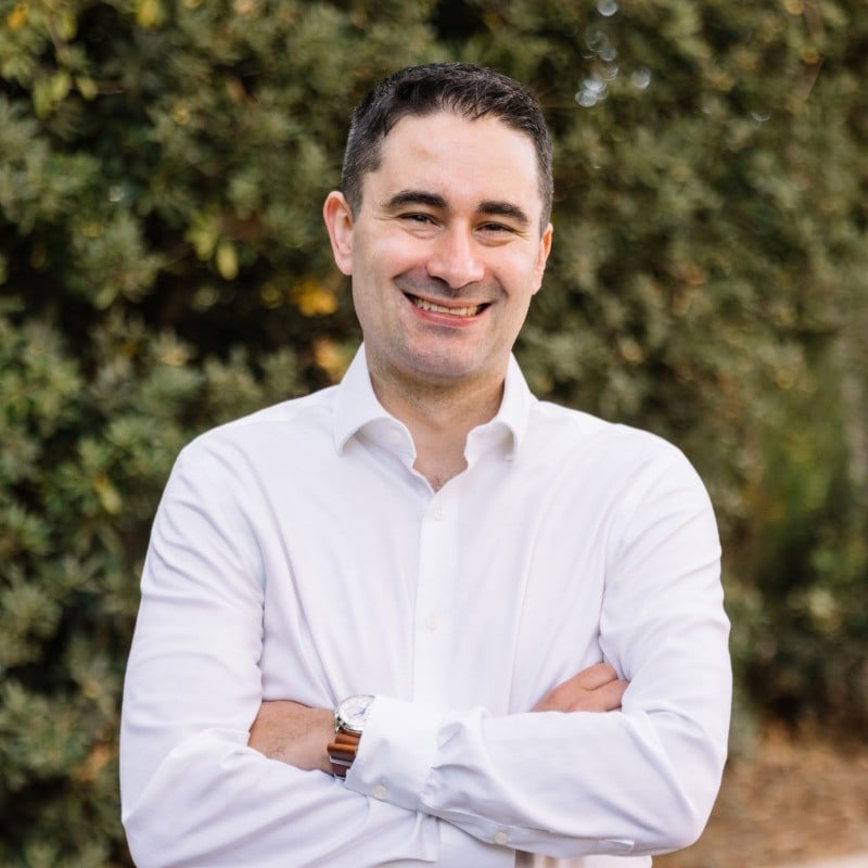
Brendan is Research Director, Semiconductors, Supply Chain, and Emerging Tech. He advises clients on strategic initiatives and leads the Futurum Semiconductors Practice. He is an experienced tech industry analyst who has guided tech leaders in identifying market opportunities spanning edge processors, generative AI applications, and hyperscale data centers.
Before joining Futurum, Brendan consulted with global AI leaders and served as a Senior Analyst in Emerging Technology Research at PitchBook. At PitchBook, he developed market intelligence tools for AI, highlighted by one of the industry’s most comprehensive AI semiconductor market landscapes encompassing both public and private companies. He has advised Fortune 100 tech giants, growth-stage innovators, global investors, and leading market research firms. Before PitchBook, he led research teams in tech investment banking and market research.
Brendan is based in Seattle, Washington. He has a Bachelor of Arts Degree from Amherst College.