The Six Five team discusses the IBM and Albany NanoTech High-EUV.
If you are interested in watching the full episode you can check it out here.
Disclaimer: The Six Five Webcast is for information and entertainment purposes only. Over the course of this webcast, we may talk about companies that are publicly traded and we may even reference that fact and their equity share price, but please do not take anything that we say as a recommendation about what you should do with your investment dollars. We are not investment advisors and we ask that you do not treat us as such.
Transcript:
Patrick Moorhead: So let me step back real quick. So most of you probably know IBM as an enterprise solution provider powerhouse. They have the full stack going all the way from quite frankly, the deepest, the hardest type of science that relates to semiconductors up through full solutions and services for Fortune 500 enterprises and big governments. They are an absolute leader in the science of what it takes to do next generation semiconductors. And you may be like, well, wait a second, Pat, it’s not the name that I think of. Well, companies like Intel, Samsung, Micron, all license technology and have collaborations with IBM. And in fact, when I was an executive at AMD, we collaborated with them on a new substrate like Silicon Insulator and new interconnects that were copper versus lead.
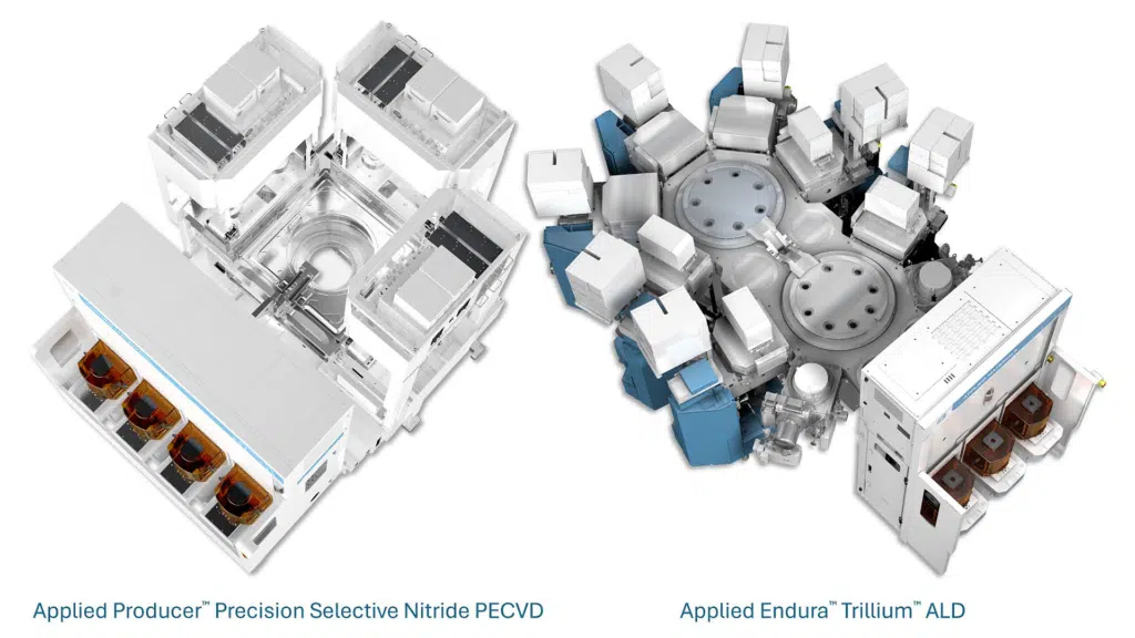
So what they’re doing in this announcement is they essentially rejoined forces with Albany NanoTech. And Dan, you and I visited that facility this year, it’s truly awesome. And think of this as a campus with the right scientists and the right machines to do this type of technology. And whatever intellectual property that the companies put in that they get out. But this arrangement was specifically around a 10 billion dollar investment into what’s called high-NA EUV. So we know what EUV is. Essentially, think of it as a two-story laser beam that does the etches on the wafer, which is just amazing. Because I don’t know how it works, but essentially adjoins atoms in the air and the laser spreads out what needs to be etched on the wafer. It is truly an incredible thing. So now we’re in this, again quote unquote two nanometers. And by the way, there’s not a single circuit that has a gate length of two nanometer, but that’s what we’re calling it now as the industry gets even harder.
So it’s not just EUV that you need, it’s high-EUV and with high-EUV you get more definition to make the circuits smaller. And I think the theory is is that you have to have less passes of the EUV laser in order to do the etching. So the partners in this one were IBM, Micron, Applied Materials, and Tokyo Electron. So what we’re going to see here is technology that gets created, and then slowly gets moved into production, licensed by companies using this technology. And you can do design, you can take something, this isn’t for high volume manufacturing. This doesn’t compete with TSMC and this doesn’t compete with let’s say the Columbus installation that Intel puts in, but it’s a great proof point on showing essentially another example of IBM’s full stack capability.
Daniel Newman: Yeah, Pat, and by the way, everybody should read the link. There’s a lot here. And Pat, you and I have a lot of semiconductor conversations with the Leading Business Press, Tech Press because of the expertise that our collective firms bring, but this stuff does get pretty geeky. What I hear here, by the way, and they say is there any hear here is that this is another example of IBM continuing to invest substantially and show leadership in the marketplace. As we move to these lower and lower numerical transistor, different numbers, two nanometer, 20 inch, from 18, you’re going to go down and down and down. And by the way, there’s really only a couple of companies in the world that are going to be enablers here.
So one of the things you like to always talk about, Pat, is kind of the research and development, the difference of R and D. There aren’t that many companies doing the kind of research that needs to be done, but for us to really get to the nano level of what’s going to be the future for continued efficiency and power gains, we need more investment in the research. And by the way, in case anybody’s wondering, the ability for the US and for Ally nations to stay on top of win the world’s economically defense-wise, security and privacy-wise is going to depend on us continuing to maintain leadership in process technology.
So we’ll talk about that more when we talk about Intel later. We’ll be talking about it here, there aren’t very many companies making these kinds of investments. This is a very important collective of companies that are coming together. And of course, this is another example, like I said, of where IBM, although they don’t get a lot of credit for being a semi company is doing a lot of really important things. And by the way, when you saw announcements like two nanometer, what? A year ago, two years ago now? I’m trying to remember. It feels like we did it on the show. Did we do it on the show?
Patrick Moorhead: Yeah, we did. Yeah. IBM had an announcement of them doing a two nanometer SRAM.
Daniel Newman: Yeah, I love that you quoted it. But anyways, with what is going on with EUV, what is going on with process node advancement, what is going on with the need to create next generation nodes and of course to gain and lead economic worldwide. And Pat, one more thing, I just want to say this in case anybody wondered, semiconductors will heat the world. I said that first in 2019 on MarketWatch. Sorry, it was important that I got that in on this show. Pat, I think it’s important that you spend the rest of the day finding an older published article where you said that, otherwise I will take claim to this.
Patrick Moorhead: I already fired up all my resources, Dan, like all 30 just to find this. So it’s a great use of my company resources.
Daniel Newman: As our show continues to get better, you’re going to start to see the onion of Patrick and my relationship exposed throughout these various topics. But anyways, good on IBM. It’s good to see these groups coming together, important work on the research side and we will probably hear more about this in the coming year.
Author Information

Daniel is the CEO of The Futurum Group. Living his life at the intersection of people and technology, Daniel works with the world’s largest technology brands exploring Digital Transformation and how it is influencing the enterprise.
From the leading edge of AI to global technology policy, Daniel makes the connections between business, people and tech that are required for companies to benefit most from their technology investments. Daniel is a top 5 globally ranked industry analyst and his ideas are regularly cited or shared in television appearances by CNBC, Bloomberg, Wall Street Journal and hundreds of other sites around the world.
A 7x Best-Selling Author including his most recent book “Human/Machine.” Daniel is also a Forbes and MarketWatch (Dow Jones) contributor.
An MBA and Former Graduate Adjunct Faculty, Daniel is an Austin Texas transplant after 40 years in Chicago. His speaking takes him around the world each year as he shares his vision of the role technology will play in our future.