Analyst(s): Brendan Burke
Publication Date: March 11, 2026
Applied Materials and Micron have formalized a joint development partnership at Applied’s new $5 billion EPIC Center in Silicon Valley to co-engineer next-generation materials for advanced DRAM, HBM, and NAND. The partnership reflects a structural shift in memory innovation, where HBM performance gains now depend less on lithographic shrink and more on novel materials architectures and precision metrology that determine bandwidth, power efficiency, and die stackability.
What is Covered in This Article:
- Applied Materials–Micron joint lab targeting materials for advanced DRAM nodes
- Why HBM scaling now hinges on materials engineering rather than dimensional shrink
- The supply-demand imbalance in HBM and its ripple effects on conventional DRAM
- Micron’s competitive positioning against SK Hynix and Samsung in the HBM market
- Whether co-located R&D models can compress the timeline from materials discovery to volume HBM production
The News:
Applied Materials and Micron Technology announced a partnership to co-develop next-generation materials engineering solutions for advanced DRAM, high-bandwidth memory (HBM), and NAND storage for AI applications. The collaboration brings together Applied’s new EPIC (Equipment and Process Innovation and Commercialization) Center in Silicon Valley and Micron’s innovation center in Boise, Idaho, creating what the companies describe as a lab-to-fab pipeline for accelerating materials research into production-ready manufacturing. The EPIC Center represents Applied Materials’ largest-ever U.S. investment in semiconductor equipment R&D, with capital spending expected to scale to approximately $5 billion as customer projects commence. Micron joins as a founding partner. The partnership scope extends beyond DRAM node transitions to include advanced packaging development for high-bandwidth, low-power memory solutions targeting power-intensive AI workloads.
Gary Dickerson, President and CEO of Applied Materials, stated: “We are excited to deepen our collaboration with Micron as a founding partner at the EPIC Center as next-generation memory technologies play an increasingly vital role in the future of AI systems.”
Sanjay Mehrotra, Chairman, President, and CEO of Micron Technology, added: “Micron has collaborated with Applied Materials for decades to deliver materials engineering innovations for new memory and storage devices, and we are pleased to extend this partnership to Applied’s new EPIC Center in Silicon Valley.”
Can Applied Materials and Micron Crack the Materials Barrier Holding Back HBM?
Analyst Take: This partnership arrives at a moment when the memory industry faces a structural paradox: the AI infrastructure buildout is generating unprecedented demand for high-bandwidth memory, yet the process technology required to sustain HBM node migration is reaching the limits of conventional scaling approaches. Each generation of GPU and XPU demands not just more memory capacity but higher bandwidth and lower power per bit, and it is these specifications that are now gated by materials innovation rather than photolithographic resolution. The Applied Materials–Micron partnership is therefore best understood not as a routine equipment qualification exercise, but as a strategic response to the deepening interdependence between memory process technology and the viability of next-generation AI compute.
HBM Scaling Has Become a Materials and Metrology Problem
Micron’s pioneering transition from 1-beta to 1-gamma DRAM represents a fundamental break from traditional memory scaling. Where prior generations relied primarily on reducing cell dimensions through improved lithographic patterning, the 1-gamma node requires entirely new high-performance dielectrics to store charge more efficiently in smaller capacitor cells, new metals such as ruthenium and molybdenum to replace conventional tungsten wiring that can no longer carry sufficient current at shrinking dimensions, and new barrier layers to prevent these materials from degrading over time. Applied Materials has positioned itself as the primary enabler of this materials transition, and its EPIC Center model is designed to compress the typically years-long gap between demonstrating a new material in the lab and integrating it into a production-worthy process flow.
For HBM specifically, this materials challenge is compounded by the unique demands of die stacking. Each DRAM die in an HBM stack must be thinned to roughly 30 microns—thinner than a human hair—and then bonded using thousands of through-silicon vias (TSVs) and micro-bump connections. At HBM3E’s twelve-high configuration, and HBM4’s planned sixteen-high stacks, the cumulative yield loss from any single defective die propagates across the entire module.
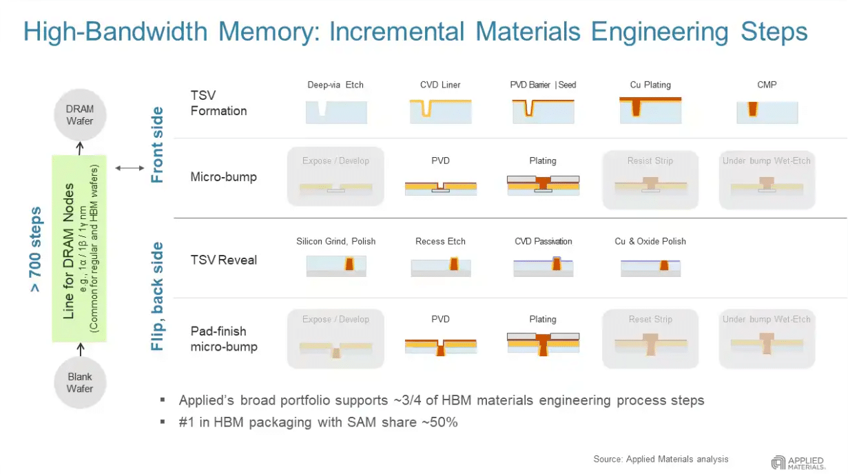
Applied Materials has highlighted that these stacking requirements demand not only better materials but fundamentally better process control and inspection capabilities. The company’s eBeam metrology systems, which can detect sub-nanometer defects invisible to optical inspection, have become essential for qualifying each DRAM die before it enters the bonding process. A single buried defect in a capacitor dielectric or an interconnect void that would be tolerable in a standalone DRAM module becomes a yield-killing failure when multiplied across a twelve- or sixteen-die HBM stack. This means the partnership’s scope likely extends beyond materials development into the metrology and inspection workflows that determine whether those materials can be manufactured at scale with acceptable yields.
The HBM Supply-Demand Imbalance Intensifies the Urgency
The commercial context for this partnership is defined by a memory market in which HBM demand has consistently outstripped supply, with cascading effects on the broader DRAM ecosystem. HBM supply constraints have persisted throughout 2024 and 2025, with memory makers allocating increasing shares of DRAM wafer capacity to HBM production, driving up spot pricing across the industry. AI chip shipments have grown at extraordinary rates over the past several quarters, and each successive generation of accelerator requires substantially more HBM per package. HBM4, expected in volume by late 2025 or early 2026, will push to sixteen-high stacks with wider interfaces, compounding the manufacturing complexity and the yield sensitivity to underlying DRAM process quality.
This dynamic creates a direct commercial incentive for Micron to accelerate its DRAM node roadmap. Faster qualification of 1-gamma and subsequent nodes translates to higher-yielding HBM stacks, improving cost per bit and competitive positioning against SK Hynix, which currently leads the HBM market in volume and qualification timelines. The Applied Materials partnership gives Micron a structural mechanism to compress the cycle between materials research and production readiness, which is precisely the bottleneck that separates HBM market share leaders from followers.
Micron’s Competitive Position in the HBM Hierarchy
The HBM market is effectively a three-player race among SK Hynix, Samsung, and Micron, with SK Hynix holding a commanding lead in both production volume and customer qualification for NVIDIA’s highest-performance platforms. Micron shipped the industry’s first 1-gamma DRAM in late 2024 and has been expanding its HBM3E supply to data center customers, but it remains the smallest of the three suppliers by HBM revenue share. Samsung, meanwhile, has struggled with HBM3E yield issues and qualification delays that have cost it design wins with NVIDIA.
For Micron, the Applied Materials partnership represents an attempt to shift the competitive dynamic by attacking the problem at the materials level. If the company can develop and qualify advanced node DRAM faster than rivals, it can produce thinner, more power-efficient dies that yield better in HBM stacks, potentially closing the gap with SK Hynix on both cost and performance. The EPIC Center model’s co-location approach is designed to eliminate the lag between when an equipment vendor develops a new deposition or etch capability and when a memory maker integrates it into a production-qualified flow.
Whether this translates into a measurable competitive advantage depends on execution. The history of semiconductor partnerships is littered with joint development agreements that produced research results but failed to accelerate production timelines. The differentiating factor here may be the specificity of the arrangement with a dedicated lab, embedded engineering teams, and a shared focus on a defined set of materials challenges, rather than a broad framework agreement.
What to Watch:
- SK Hynix holds around 60% of the global HBM market and has already begun mass production of HBM4, meaning any materials engineering breakthroughs from this partnership must close a significant technology and volume gap before they translate into competitive repositioning for Micron.
- Micron’s ability to sustain leadership at the leading DRAM node will depend on whether the EPIC Center co-development model can compress the cycle between materials discovery and production-ready integration faster than SK Hynix and Samsung achieve through their own internal R&D programs.
- The transition to HBM4’s sixteen-high die stacks introduces compounding yield challenges in advanced packaging that sit outside the scope of this DRAM-focused partnership, meaning materials engineering alone may not resolve the full manufacturing bottleneck.
- Applied Materials’ ability to scale its EPIC Center collaborative model across multiple memory customers without creating exclusivity conflicts will determine whether the insights generated with Micron translate into broader equipment revenue or remain a single-customer engagement.
See the complete press release on the Applied Materials and Micron partnership to advance DRAM innovation on the Applied Materials investor relations website.
Disclosure: Futurum is a research and advisory firm that engages or has engaged in research, analysis, and advisory services with many technology companies, including those mentioned in this article. The author does not hold any equity positions with any company mentioned in this article.
Analysis and opinions expressed herein are specific to the analyst individually and data and other information that might have been provided for validation, not those of Futurum as a whole.
Other Insights from Futurum:
Can Micron’s Modular Memory Upgrade Help NVIDIA’s CPUs Outperform?
Applied Materials Q1 FY 2026: AI Demand Lifts Outlook
Will Applied Materials’ Transistor Breakthroughs Empower 2nm AI Chips?
Image Credit: Applied Materials
Author Information

Brendan is Research Director, Semiconductors, Supply Chain, and Emerging Tech. He advises clients on strategic initiatives and leads the Futurum Semiconductors Practice. He is an experienced tech industry analyst who has guided tech leaders in identifying market opportunities spanning edge processors, generative AI applications, and hyperscale data centers.
Before joining Futurum, Brendan consulted with global AI leaders and served as a Senior Analyst in Emerging Technology Research at PitchBook. At PitchBook, he developed market intelligence tools for AI, highlighted by one of the industry’s most comprehensive AI semiconductor market landscapes encompassing both public and private companies. He has advised Fortune 100 tech giants, growth-stage innovators, global investors, and leading market research firms. Before PitchBook, he led research teams in tech investment banking and market research.
Brendan is based in Seattle, Washington. He has a Bachelor of Arts Degree from Amherst College.