Qualcomm validated its first-generation High Bandwidth Compute silicon, measuring an 18x memory bandwidth gain over LPDDR and 5x bandwidth per watt over HBM4 on a two-layer DRAM test sample. Futurum examines whether stacked DRAM on compute can beat custom HBM to the inference socket.
What Is Covered in This Article:
- First-generation HBC silicon validated in Qualcomm’s lab after more than a month of testing
- A live tester demo measuring an 18x memory bandwidth gain over LPDDR and 5x bandwidth per watt over HBM4
- A two-layer stacked DRAM validation sample ahead of a four-layer production stack in AI250
- AI250 and the Dragonfly C1000 CPU sampling in the first half of 2027, with Gen 2 HBC and AI300 in 2028
- HBC as a Qualcomm product spanning data center, automotive, PC, XR, and Snapdragon platforms
The News: Qualcomm announced that its first-generation High Bandwidth Compute (HBC) silicon has been validated in the lab, converting the near-memory architecture it unveiled at its June 2026 investor day into measured hardware. The validation sample, a two-layer stacked DRAM with an AI accelerator die bonded underneath, has run on a test system for more than a month and Qualcomm showed a recorded demo of it in a pre-briefing attended by Futurum. Running the same workload in LPDDR mode and then in HBC mode, the sample measured an 18x memory bandwidth advantage and Qualcomm reported 5x better bandwidth per watt than HBM4, consistent with the figures it presented in June.
“This is not a normal chip. This is the first time that somebody has done something like this,” said Gerardo Giaretta, Vice President and General Manager of Qualcomm’s data center CPU and AI business unit.
The production version will stack four DRAM layers, and the Dragonfly AI250, the first platform built on HBC, has entered full bring-up and will sample to customers in the first half of 2027 alongside the C1000 data center CPU, with second-generation HBC arriving in the AI300 in 2028. Giaretta said Qualcomm is working with multiple customers on HBC implementations beyond the AI250 program.
Qualcomm Validates First HBC Silicon With an 18x Memory Bandwidth Gain Over LPDDR5X
Analyst Take: HBC validation is the proof point Qualcomm’s data center reentry needed most. The company’s case for entering a market NVIDIA, AMD, and a field of custom silicon programs already occupy rests on one architectural wager, that stacking DRAM directly on an AI accelerator dismantles the “memory wall” throttling transformer decode, and until now that wager existed as presentation slides. A two-layer sample on a tester proves the architecture and the wafer-on-wafer bonding. It does not yet prove that a four-layer stack yields economically at the gigawatt scale Qualcomm intends to supply. The decode-dominated inference era Futurum has tracked across its 2026 coverage rewards exactly the bandwidth-per-dollar profile HBC claims, so the next two quarters of yield and benchmark disclosures will decide whether Qualcomm has built a differentiated franchise or an elegant prototype.
Lab Silicon Converts HBC From Investor Day Promise to Measured Data
The demo was deliberately simple. Qualcomm placed a standalone HBC device on a tester, pushed weights and activations from a host, and ran the inference task twice, once over a conventional LPDDR path and once with computation executing in the logic die beneath the DRAM stack. The 18x gain is a measured result on working silicon, though Qualcomm did not disclose the workload, nor the model, precision, or batch size, so the figure reflects a component kernel rather than end-to-end inference.
The energy savings follow from physics, since data traveling micrometers through vertical bonds consumes an order of magnitude less power than data crossing a package. Futurum asked whether the efficiency claim had slipped from June’s 6x versus HBM to the demo’s 5x versus HBM4, and Giaretta answered that the result ranges from 5x to 6x depending on normalization, with nothing in testing changing the June claims. Both figures remain Qualcomm-supplied, measured on a two-layer sample rather than the production stack.
Yield is the harder question. Stacked architectures multiply yield losses, since a defect in any DRAM layer or the logic die compromises the package, and Giaretta acknowledged the point while citing repairability as a core piece of Qualcomm’s R&D. The next proof point is no longer architectural. It is a yield curve.
HBC Puts an Accelerator Where Custom HBM Puts a Memory Controller
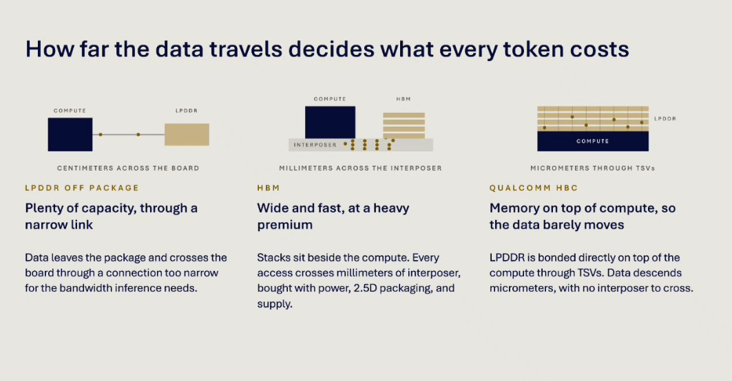
HBC is on a collision course with the custom HBM the memory vendors are selling to every XPU program. In a September Futurum briefing, In Futurum’s assessment, custom HBM is a through-silicon via story. The vias feeding a DRAM stack consume base-die area and act as thermal pillars, which is why custom HBM base dies have so far added memory controllers and repair logic rather than meaningful compute. Qualcomm claims a connection-level innovation that frees that real estate for serious accelerator logic, and the same briefing estimated that HBM plus I/O can consume up to 50% of an XPU’s power budget, the cost HBC removes.
Durga Malladi, Qualcomm Fellow and EVP and GM of technology planning for edge solutions and data center, told Austin Lyons of Chipstrat that memory vendors responded to the concept by asking to work closer with Qualcomm, and several have announced stacked-DRAM variants of their own, including Samsung’s zHBM, which Futurum covered in its October analysis. Malladi said stacked DRAM and customized HBM “will co-evolve for a period of time and we’ll see what happens after that.”
Qualcomm argues HBC is superior in technical framing and complementary in public posture. The open question is whether any Qualcomm roadmap product will ship custom HBM4E or whether HBC answers that socket across the portfolio, down to a potential Snapdragon platform. The cited 133 TB/s for HBC Gen 1 deserves careful reading. That figure sums the bandwidth across the vertical bonds between the DRAM stack and the compute die inside the package, while the roughly 3.3 TB/s it is compared against is what a single HBM4 stack delivers over its external interface to a separate processor. An XPU mounts 6 to 8 HBM4 stacks, so the aggregate bandwidth reaching a GPU’s compute is on the order of 20 to 27 TB/s, which shrinks the headline 40x gap to roughly 5x to 7x at the package level. HBC’s advantage remains real since the data sits directly on compute without crossing an interposer.
Decode Economics and Manufacturing Scale Will Decide Whether HBC Wins Sockets
What to Watch:
- Whether the four-layer production stack reaches high-yield manufacturing ahead of AI250 sampling in the first half of 2027
- Whether Qualcomm publishes end-to-end tokens per second per watt on AI250 racks rather than component-level bandwidth figures
- Whether a hyperscaler beyond Humain commits publicly to AI250 or HBC-based deployments in 2027
- Whether custom HBM4E base dies gain compute functions beyond controllers and repair logic, narrowing HBC’s claimed advantage
- Whether Samsung zHBM, SK hynix AI-DRAM, and other memory-vendor stacked DRAM variants align with Qualcomm’s supply chain or compete against it
Read the complete announcement on the HBC silicon validation on the Qualcomm website.
Sources
- Qualcomm HBC demonstrates AI inference leadership with validated silicon, Qualcomm, November 2026
Declaration of generative AI and AI-assisted technologies in the writing process: This content has been generated with the support of artificial intelligence technologies. Due to the fast pace of content creation and the continuous evolution of data and information, The Futurum Group and its analysts strive to ensure the accuracy and factual integrity of the information presented. However, the opinions and interpretations expressed in this content reflect those of the individual author/analyst. The Futurum Group makes no guarantees regarding the completeness, accuracy, or reliability of any information contained herein. Readers are encouraged to verify facts independently and consult relevant sources for further clarification.
Disclosure: Futurum is a research and advisory firm that engages or has engaged in research, analysis, and advisory services with many technology companies, including those mentioned in this article. The author does not hold any equity positions with any company mentioned in this article.
Analysis and opinions expressed herein are specific to the analyst individually and data and other information that might have been provided for validation, not those of Futurum as a whole.
Read the full Futurum Group Disclosure.
Other Insights From Futurum:
Qualcomm Wins Liability Verdict Against Arm With Royalty Suspension Ruling To Follow
Qualcomm + PickNik + Layoffs = The Robotics Segment’s Stakes Are Starting To Feel A Bit More Real
Snapdragon X Elite Expands Qualcomm’s PC Reach With Googlebook
Author Information

Brendan is Research Director, Semiconductors, Supply Chain, and Emerging Tech. He advises clients on strategic initiatives and leads the Futurum Semiconductors Practice. He is an experienced tech industry analyst who has guided tech leaders in identifying market opportunities spanning edge processors, generative AI applications, and hyperscale data centers.
Before joining Futurum, Brendan consulted with global AI leaders and served as a Senior Analyst in Emerging Technology Research at PitchBook. At PitchBook, he developed market intelligence tools for AI, highlighted by one of the industry’s most comprehensive AI semiconductor market landscapes encompassing both public and private companies. He has advised Fortune 100 tech giants, growth-stage innovators, global investors, and leading market research firms. Before PitchBook, he led research teams in tech investment banking and market research.
Brendan is based in Seattle, Washington. He has a Bachelor of Arts Degree from Amherst College.