Analyst(s): Brendan Burke
Publication Date: May 7, 2026
Applied Materials has agreed to acquire ASMPT Limited’s NEXX business, a supplier of large-area electrochemical deposition equipment for advanced semiconductor packaging. The deal strengthens Applied’s position in panel-level processing, a substrate format increasingly critical to building the larger, more complex AI accelerator packages that chipmakers and systems companies require.
What is Covered in This Article:
- Applied Materials’ acquisition of NEXX from ASMPT Limited
- Panel-level packaging’s role in scaling AI accelerator architectures
- Strategic fit between electrochemical deposition and Applied’s existing tool portfolio
- Competitive dynamics in a consolidating packaging equipment market
- Execution considerations as panel-level processing nears volume production
The News: Applied Materials announced on May 3, 2026, that it has entered into a definitive agreement with ASMPT Limited to acquire its NEXX business, a leading supplier of large-area advanced packaging deposition equipment for the semiconductor industry. The NEXX team and product line will join Applied’s Semiconductor Products Group and continue to operate from Billerica, Massachusetts, following the transaction’s expected close within the next several months, subject to customary closing conditions with no regulatory approvals required. The acquisition adds panel-level electrochemical deposition (ECD) technology to Applied’s existing advanced packaging portfolio, which already spans digital lithography, physical vapor deposition (PVD), chemical vapor deposition (CVD), etch, and eBeam metrology and inspection.
“Having NEXX join Applied Materials complements our leadership in advanced packaging, particularly in panel processing — an area where we see tremendous opportunities for customer co-innovation and growth in the years ahead,” said Dr. Prabu Raja, President of the Semiconductor Products Group at Applied Materials.
Applied Materials Targets Panel-Level Packaging Gap With NEXX Acquisition
Analyst Take: Applied Materials’ acquisition of NEXX signals a deliberate effort to consolidate panel-level advanced packaging capabilities at a moment when AI accelerator architectures are driving urgent demand for larger substrates and denser interconnects. TSMC’s CoPoS (Chips on Panel on Substrate) pilot line is expected to be completed in mid-2026, with volume ramp targeted around 2028–2029, while Silicon Box shipped 100 million panel-level packaging units from its Singapore facility in October 2025, proving the form factor’s production viability. By adding electrochemical deposition to a portfolio that already covers lithography, PVD, CVD, etch, and metrology, Applied is positioning itself as a single-source provider for panel-level advanced packaging equipment at precisely the moment the transition moves from pilot to production. The question facing Applied is whether the breadth of the portfolio translates into depth of adoption as chipmakers navigate an unfamiliar substrate format under intense time pressure.
Electrochemical Deposition Fills a Critical Process Gap
Applied Materials has built its panel-level packaging portfolio through internal development of its Topaz PVD system — capable of processing substrates up to 600 by 600 millimeters — and related lithography, CVD, and etch platforms, but electrochemical deposition represents a distinct process step where the company lacked a leading market position. ECD is essential for fine-pitch I/O wiring and redistribution layer metallization on large-format substrates, processes that become more demanding as interconnect density increases with each generation of AI accelerator design. NEXX’s specialization in large-area ECD for advanced packaging means Applied acquires not only hardware but also process knowledge tuned to substrates well beyond conventional wafer dimensions.
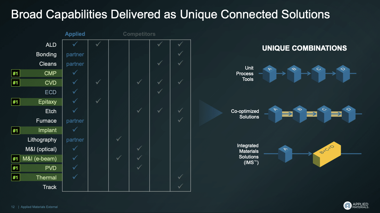
The combination enables Applied to offer co-optimized deposition stacks — PVD seed layers from the Topaz system, followed by ECD copper fill — on the same panel format without requiring customers to qualify equipment from multiple vendors. This matters because process integration at panel scale introduces variables in thermal management, uniformity, and alignment that compound when equipment comes from different suppliers with different specifications. Applied can now offer chipmakers a more tightly coupled process flow, reducing the qualification burden during a substrate transition that is already technically challenging.
Panel-Level Processing as an AI Infrastructure Imperative
The transition from 300-millimeter wafer-level processing to panel form factors exceeding 510×515 millimeters is a structural requirement as 2.5D and 3D chiplet designs scale to integrate greater numbers of XPUs, high-bandwidth memory stacks, and I/O chips in a single package. Applied Materials estimated ECD’s market size as part of a category contributing 3% of the $115 billion CY25 wafer fabrication equipment market, or $3.5 billion. TSMC has explicitly indicated a roadmap to 9.5-reticle-size CoWoS in volume production by 2027, and its next-generation CoPoS platform adopts a square panel design at initial specifications of 310×310 millimeters, with future scalability to 510×515 millimeters or larger. The normalized capital cost advantage of panel-level processing over wafer-level formats — which Applied has previously characterized as more than a two-to-one reduction — creates strong economic incentives for chipmakers to adopt the new form factor.
However, the entire equipment ecosystem must mature simultaneously, as no single tool vendor can force the transition alone. Applied’s Topaz PVD system already demonstrated capabilities such as low contact resistance, double the minimum required adhesion strength, conformal seed layers with excellent sidewall coverage, and substrate temperatures below 120 degrees Celsius on panels up to 600 by 600 millimeters. The takeaway is that Applied is betting its breadth of panel-level capability will accelerate an industry transition whose urgency is set by AI accelerator roadmaps, not by equipment vendor readiness.
Market Consolidation Before the Volume Inflection
Applied Materials explicitly notes that the NEXX acquisition broadens its served addressable market, a signal that the company views organic development as insufficient to capture the panel-level opportunity within the required timeframe. Competitors such as Lam Research and Tokyo Electron remain strong in core process equipment but lack comparable integrated panel-level packaging ecosystems, giving Applied a window to establish a dominant position before the market reaches volume scale. The carve-out structure, with NEXX continuing as a distinct team in Billerica, suggests Applied intends to preserve the acquired expertise and customer relationships rather than absorb them into existing operations.
The absence of regulatory approval requirements indicates the relative nascency of the panel-level market — it has not yet reached the scale where equipment consolidation triggers antitrust scrutiny. Meanwhile, new entrants such as SCHMID Group are introducing complementary panel-level processes, including electrochemical etch technologies for advanced substrates, signaling that the competitive window for establishing leadership remains open but is narrowing. Applied is moving to secure a dominant portfolio position in panel-level equipment before the market matures enough for such consolidation to attract meaningful competitive or regulatory response.
Execution Risk in a Pre-Volume Market
The panel-level packaging market’s high growth reflects expected demand rather than current production volumes, and the primary advanced packaging volumes today remain in 2.5D packages built on 300mm wafer-sized interposers. Applied must integrate NEXX’s ECD technology and demonstrate co-optimized process flows with its existing Topaz PVD, CVD, and lithography tools before chipmakers commit to volume-scale panel-level production lines. Silicon Box’s 100-million-unit shipment milestone from its Singapore facility proves that panel-level processing can achieve production-grade yields, but the transition from fan-out packaging to the high-density interposer applications demanded by AI accelerators introduces substantially greater process complexity.
The carve-out integration model — preserving NEXX as a distinct team within Applied’s Semiconductor Products Group — reduces short-term disruption risk but creates longer-term questions about how tightly NEXX’s technology will be co-optimized with Applied’s adjacent tools. Customers evaluating panel-level production lines will weigh Applied’s breadth of portfolio against demonstrated co-optimization results on production substrates, not marketing claims about integrated capability. Applied’s acquisition thesis depends on rapid execution during a narrow window between pilot-line qualification and volume ramp, where delays could allow competitors or alternative architectures to establish footholds.
What to Watch:
- Whether AI chipmakers accelerate panel-level pilot programs following Applied’s expanded portfolio availability.
- TSMC’s CoPoS pilot line completion timeline and its implications for panel-level equipment demand signaling.
- How quickly Applied demonstrates co-optimized PVD-to-ECD process flows on production-scale panel substrates.
- The degree to which competing equipment vendors such as Lam Research and Tokyo Electron respond with their own panel-level acquisitions or partnerships.
- Whether the carve-out integration model preserves NEXX’s development velocity or introduces coordination friction with Applied’s existing panel-level tools.
See the full press release on Applied Materials’ NEXX acquisition announcement on the company website.
Disclosure: Futurum is a research and advisory firm that engages or has engaged in research, analysis, and advisory services with many technology companies, including those mentioned in this article. The author does not hold any equity positions with any company mentioned in this article.
Analysis and opinions expressed herein are specific to the analyst individually and data and other information that might have been provided for validation, not those of Futurum as a whole.
Other Insights From Futurum:
Applied Materials Arms Chipmakers for the GAA Era With Angstrom-Class Tools
Can Applied Materials and Micron Crack the Materials Barrier Holding Back HBM?
Applied Materials Q1 FY 2026: AI Demand Lifts Outlook
Author Information

Brendan is Research Director, Semiconductors, Supply Chain, and Emerging Tech. He advises clients on strategic initiatives and leads the Futurum Semiconductors Practice. He is an experienced tech industry analyst who has guided tech leaders in identifying market opportunities spanning edge processors, generative AI applications, and hyperscale data centers.
Before joining Futurum, Brendan consulted with global AI leaders and served as a Senior Analyst in Emerging Technology Research at PitchBook. At PitchBook, he developed market intelligence tools for AI, highlighted by one of the industry’s most comprehensive AI semiconductor market landscapes encompassing both public and private companies. He has advised Fortune 100 tech giants, growth-stage innovators, global investors, and leading market research firms. Before PitchBook, he led research teams in tech investment banking and market research.
Brendan is based in Seattle, Washington. He has a Bachelor of Arts Degree from Amherst College.