Analyst(s): Brendan Burke
Publication Date: April 9, 2026
Applied Materials has unveiled two new chipmaking systems — Precision Selective Nitride PECVD and Trillium ALD — engineered to deposit metals and dielectrics at atomic-scale tolerances inside Gate-All-Around transistors at 2nm and below. The announcement underscores a broader industry inflection in which materials engineering, rather than lithography alone, is becoming the primary lever for sustaining transistor performance gains in the AI compute era.
What is Covered in This Article:
- Applied Materials’ two new deposition systems for angstrom-era GAA transistors
- The shift from lithography-led scaling to materials-driven performance gains
- Implications of GAA complexity for wafer fabrication equipment spending mix
- Applied’s positioning across a multi-foundry, multi-architecture landscape
- Logic-like complexity entering memory fabrication and the HBM convergence
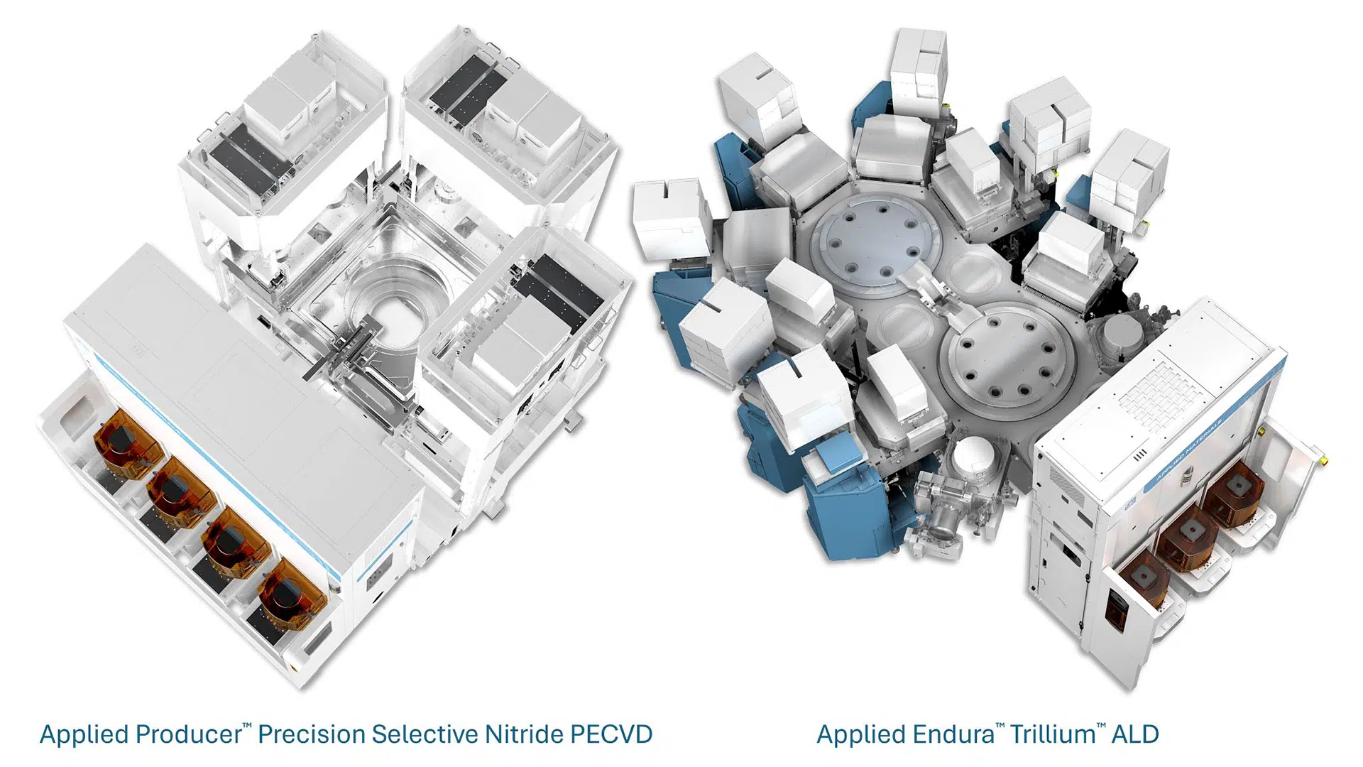
The News: Applied Materials introduced two chipmaking systems on April 8, 2026, designed to create the smallest features in the most advanced logic chips currently in production. The two systems — the Applied Producer Precision Selective Nitride PECVD (Plasma Enhanced Chemical Vapor Deposition) system and the Applied Endura Trillium ALD (Atomic Layer Deposition) system — target deposition challenges specific to Gate-All-Around (GAA) transistor architectures at the 2nm node and beyond. The Precision Selective Nitride PECVD system uses a selective bottom-up deposition process to place a dense silicon nitride layer atop silicon oxide within shallow trench isolation (STI) structures. The Trillium ALD system is an Integrated Materials Solution designed to deposit complex metal gate stacks that control the threshold voltage of GAA transistors.
Dr. Prabu Raja, President of Applied Materials’ Semiconductor Products Group, stated that the industry is “entering a period of rapid, non-linear change” in which “traditional lithographic chip scaling alone is no longer sufficient.” He noted that “at the most advanced angstrom-class logic nodes, performance and power are increasingly determined by materials.”
Applied disclosed the announcements ahead of its Logic Master Class event held on the same day. The company framed the broader context as a $115 billion wafer fabrication equipment (WFE) market in which the spending mix is shifting toward leading-edge logic and memory. Building a single GAA transistor now requires more than 500 process steps, many of which demand entirely new deposition methods operating within tolerances approaching the size of individual atoms.
Applied Materials Arms Chipmakers for the GAA Era With Angstrom-Class Tools
Analyst Take: Applied Materials’ announcement arrives at a moment when the semiconductor industry’s center of gravity is visibly shifting. For decades, lithographic patterning — the ability to print ever-smaller features onto silicon — was the primary mechanism through which chipmakers advanced transistor density and performance. That dynamic is changing.
The transition from FinFET to GAA transistor architectures at 2nm introduces a step-function increase in three-dimensional structural complexity that lithography alone cannot address. With more than 500 process steps required to fabricate a single GAA transistor, the ability to deposit metals and dielectrics at atomic-scale precision — and to do so repeatably across billions of transistors — has become the binding constraint on node progression. This is the strategic thesis underlying both the Precision Selective Nitride and Trillium ALD systems.
Applied positions materials engineering as the primary enabler of continued scaling at a time when chipmakers can extract meaningful performance gains from GAA architectures at 2nm before they transition to high-numerical-aperture extreme ultraviolet (high-NA EUV) lithography. Applied VP of Integrated Materials Solutions Bala Haran described 2nm as a “monster node” precisely because it offers a wide design space for differentiated nanosheet architectures that is defined overwhelmingly by materials choices, not patterning resolution.
A Multi-Foundry World Plays to Applied’s Breadth
One of the less obvious but strategically significant dimensions of the GAA transition is the degree of architectural divergence it introduces among foundry-logic manufacturers. Unlike FinFET, where process recipes converged across fabs over successive nodes, GAA nanosheet spacing and metal gate stack composition are being approached differently by each major foundry. Every customer is pursuing a differentiated nanosheet architecture optimized for its target workloads, whether mobile, PC, or AI accelerators.
This fragmentation creates a structural advantage for equipment vendors with broad, adaptable process platforms rather than narrow, application-specific tools. Applied’s Trillium ALD system, with its ability to integrate multiple metal deposition steps and tune threshold voltage across transistor variants on a single platform, is designed to serve precisely this kind of heterogeneous demand. If the multi-foundry thesis holds, Applied’s addressable opportunity expands with each foundry’s differentiated approach to GAA rather than contracting toward a single dominant recipe.
WFE Mix Shift Signals a Broader Rebalancing
Applied’s characterization of the WFE market at $115 billion in 2025, with the spending mix shifting toward leading-edge logic and memory, deserves scrutiny. The semiconductor industry’s WFE spending has historically been weighted toward logic, but the AI infrastructure buildout is driving a rebalancing. Memory is absorbing an increasing share of capital expenditure as chipmakers such as SK Hynix, Micron, and Samsung invest in packaging more transistors and wiring alongside DRAM arrays to make memory architecturally more “logic-like.”
Applied’s partnerships with all three major memory manufacturers at its EPIC R&D center reinforce this convergence. The implication is that the materials complexity traditionally associated with advanced logic fabrication is migrating into memory manufacturing as well, expanding Applied’s serviceable market in both segments simultaneously. Memory’s share of WFE spending stood at approximately 23% in 2023, and the trajectory of HBM investment and advanced packaging buildout suggests a meaningful increase in the near term. This dual exposure is a structural differentiator for Applied relative to equipment peers whose revenue concentration skews more heavily toward a single segment.
Valuation Disconnect Warrants Monitoring
Despite its dominant position in materials modification — a standalone market estimated at approximately $4.5 billion — and its expanding opportunities across GAA deposition, etch, and eBeam process control, Applied Materials has traded at a discount to several semiconductor equipment peers. The GAA transition, the expansion of materials-driven process steps, and the convergence of logic and memory complexity all represent secular tailwinds that may not yet be reflected in the company’s relative valuation. Whether the market reprices this positioning will depend on the pace of GAA adoption and the degree to which Applied converts its R&D leadership into production tool-of-record wins across multiple foundries. For now, the Logic Master Class disclosures suggest the technical foundation is in place. The commercial execution will determine the rest.
What to Watch:
- ASML’s ability to ramp next-generation lithography at competitive cost-per-wafer will determine how long chipmakers rely on Applied’s materials-intensive, multi-patterning approach at 2nm before shifting to a lithography-led path.
- Applied Materials’ push from deposition dominance into adjacent etch and eBeam process control invites competitive countermoves from rivals with deep GAA-optimized tooling expertise of their own.
- If memory approaches 50% of the WFE market as HBM architectures grow more logic-like, equipment demand could surge, but also strain critical subsystem supply chains.
- TSMC, Samsung, and Intel are each pursuing differentiated nanosheet architectures for GAA, which broadens Applied’s addressable market but raises the cost and complexity of supporting multiple integration schemes simultaneously.
- Sustained enterprise appetite for AI inference accelerators at established nodes means GAA adoption at 2nm will supplement rather than cannibalize FinFET equipment spending, supporting investment across both leading-edge and mature fabs.
See the complete press release on deposition systems for angstrom-era logic chips on the Applied Materials website.
Disclosure: Futurum is a research and advisory firm that engages or has engaged in research, analysis, and advisory services with many technology companies, including those mentioned in this article. The author does not hold any equity positions with any company mentioned in this article.
Analysis and opinions expressed herein are specific to the analyst individually and data and other information that might have been provided for validation, not those of Futurum as a whole.
Other Insights from Futurum:
Can Applied Materials and Micron Crack the Materials Barrier Holding Back HBM?
Applied Materials Q1 FY 2026: AI Demand Lifts Outlook
Will Applied Materials’ Transistor Breakthroughs Empower 2nm AI Chips?
Image Credit: Applied Materials
Author Information

Brendan is Research Director, Semiconductors, Supply Chain, and Emerging Tech. He advises clients on strategic initiatives and leads the Futurum Semiconductors Practice. He is an experienced tech industry analyst who has guided tech leaders in identifying market opportunities spanning edge processors, generative AI applications, and hyperscale data centers.
Before joining Futurum, Brendan consulted with global AI leaders and served as a Senior Analyst in Emerging Technology Research at PitchBook. At PitchBook, he developed market intelligence tools for AI, highlighted by one of the industry’s most comprehensive AI semiconductor market landscapes encompassing both public and private companies. He has advised Fortune 100 tech giants, growth-stage innovators, global investors, and leading market research firms. Before PitchBook, he led research teams in tech investment banking and market research.
Brendan is based in Seattle, Washington. He has a Bachelor of Arts Degree from Amherst College.