Analyst(s): Ron Westfall
Publication Date: April 23, 2025
What is Covered in this Article:
- Why Lighmatter’s photonic AI acceleration research is pivotal for the future of computing because it addresses fundamental limitations in traditional electronic computing, particularly in the context of rapidly growing AI workloads
- How Lightmatter Passage M1000 and L200 products are poised to deliver breakthroughs in photonic supercomputing due to their innovative use of 3D photonic interconnects, which address critical bottlenecks in traditional electrical interconnects for AI and HPC.
- Lightmatter’s strategic use of GlobalFoundries’ GF Fotonix platform, combined with partnerships with Amkor and ASE for packaging, significantly enhances its production readiness, supply chain resilience, and tariff-related stability.
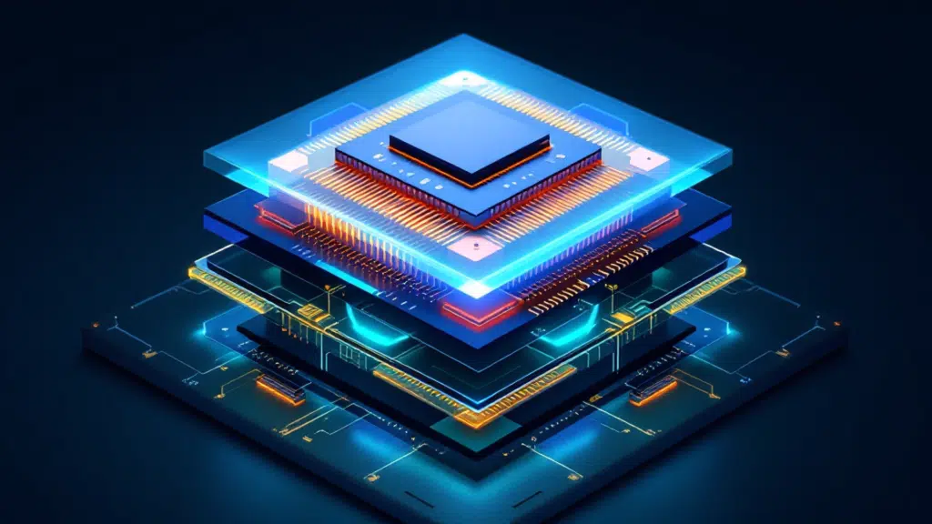
The News: At OFC25, Lightmatter announced the Passage M1000, a 3D Photonic Superchip designed for next-generation XPUs and switches, and the Passage L200, 3D co-packaged optics (CPO). Both products are integral to the company’s Passage platform, a 3D-stacked silicon photonics engine designed to connect thousands to millions of processors at the speed of light.
Lightmatter: Solving How to Interconnect Millions of Chips
Analyst Take: Lightmatter’s breakthrough photonic AI acceleration research is pivotal for the future of computing because it addresses fundamental limitations in traditional electronic computing, particularly in the context of rapidly growing AI workloads. These limitations stem from the stalling of Moore’s Law, Dennard scaling, and memory scaling, which can no longer keep pace with the exponential computational demands of AI. Lightmatter’s approach leverages photonics, using light to process and transmit data, to achieve unprecedented performance, energy efficiency, and scalability, especially for interconnecting millions of chips in large-scale AI systems.
Moore’s Law (doubling transistor density every two years) and Dennard scaling (power efficiency improvements with smaller transistors) have slowed significantly. This makes it increasingly costly and inefficient to scale traditional silicon-based chips by adding more transistors or increasing silicon area. AI workloads, which require massive matrix operations and data movement, exacerbate these issues, pushing electronic systems to their physical and energy limits.
Lightmatter gets right to solving how to interconnect millions of chips by using 3D photonic interposer technology to demonstrate sharp competitive advantages. Lightmatter’s 3D photonic interposer outperforms 2.5D by allowing I/O placement across the entire chip surface, providing exceptional bandwidth (114–256 Tbps), improving energy efficiency, and enabling flexible integration with scalable, production-ready manufacturing. These strengths overcome the interconnect challenges in AI and HPC, eclipsing the constraints of 2.5D’s edge-limited, electrically reliant designs. Utilizing 3D stacking and photonic technology, Lightmatter’s solution is ideally suited to fulfill the performance and scalability needs of next-generation AI infrastructure.
Moreover, I find that Lightmatter’s strategic use of GlobalFoundries’ GF Fotonix platform, combined with partnerships with Amkor and ASE for packaging, significantly enhances the production readiness, supply chain resilience, and tariff stability for its Passage M1000 and L200 photonic supercomputing products.
Delivering Energy Efficiency and Massive Scalability in the AI Era
Training large AI models, like those powering ChatGPT, consumes enormous energy, sometimes the equivalent to the annual energy use of hundreds of households. Data centers are hitting power walls, and the heat generated by traditional chips requires extensive cooling, further increasing costs and environmental impact.
Photonic computing generates less heat than electronic circuits because it relies on light rather than electrical current for data processing and transport. Lightmatter’s Envise chip combines photonic and electronic components to handle AI computations efficiently, while its Passage interconnect minimizes energy losses in data transfer. This dual approach reduces the energy footprint of AI infrastructure, making it more sustainable and cost-effective.
Lightmatter’s photonic processors, such as the Envise and Passage chips, use light to perform computations, particularly tensor operations central to deep learning. By manipulating light through optical components like waveguides and lenses, these chips execute calculations at the speed of light, achieving near-electronic precision while consuming significantly less power. For example, their photonic processor performs 65.5 trillion Adaptive Block Floating-Point 16-bit (ABFP) operations per second using only 78 watts of electrical power and 1.6 watts of optical power. This efficiency is critical as AI data centers are projected to consume up to 20% of global power by 2030 if current trends continue.
As AI clusters grow to include tens of thousands or even millions of accelerators (e.g., GPUs or XPUs), the computational and interconnect demands increase exponentially. Traditional electronic interconnects cannot scale efficiently due to bandwidth, latency, and power constraints.
Lightmatter’s photonic chips, particularly the recently introduced Passage series, are designed for scalability. The Passage M1000, for instance, supports multi-reticle die complexes up to 4,000 mm², integrating thousands of GPUs in a single domain with 114 Tbps of optical bandwidth. This scalability is crucial for building the massive, high-performance systems needed for future AI and high-performance computing (HPC) workloads
Lightmatter Passage Ready to Take Photonic Supercomputing to the Next Level
I find that the Lightmatter Passage M1000 and L200 products are poised to deliver breakthroughs in photonic supercomputing due to their innovative use of 3D photonic interconnects, which address critical bottlenecks in traditional electrical interconnects for AI and HPC.
The Passage M1000 offers an unparalleled 114 Tbps of total optical bandwidth, enabled by a 3D photonic interposer with 256 optical fibers and a 4,000 mm² multi-reticle design. This allows massive die complexes to connect thousands of GPUs in a single domain, far surpassing the bandwidth limitations of electrical I/O, which is restricted to chip edges, which can be understood as the “shoreline”.
The Passage L200 provides up to 256 Tbps of I/O bandwidth per chip package (with 32 Tbps and 64 Tbps versions, L200 and L200X), achieving up to 8x faster AI model training by integrating 3D co-packaged optics (CPO). This eliminates bandwidth bottlenecks, offering 5-10x improvement over existing solutions.
Both products leverage 3D integration to position electro-optical I/O across the entire chip surface, not limited to the edges. This “edgeless” design, enabled by a reconfigurable waveguide network and dense wavelength division multiplexing (DWDM), boosts bandwidth and minimizes latency compared to traditional electrical or optical solutions constrained by shoreline boundaries.
Photonic interconnects use light for data transfer, lowering power usage compared to electrical interconnects, which face issues with heat and resistance. The M1000 enables over 1.5kW power delivery, and the L200’s integration with Alphawave Semi’s energy-efficient UCIe and SerDes boosts efficiency. This scalability is essential for distributed AI clusters using millions of XPUs.
Leveraging GlobalFoundries’ GF Fotonix platform and collaborations with Amkor and ASE for packaging, these products are primed for high-volume production. The M1000 employs solid-state optical circuit switching, while the L200 incorporates Alphawave Semi’s chiplet technology, ensuring reliability and compatibility with next-generation XPUs and switches.
From my point of view, these products can facilitate faster training of larger, more advanced AI models, meeting the need for interconnects that match rapidly advancing compute performance, which has surpassed traditional scaling laws like Moore’s Law. The L200’s 200+ Tbps per package and the M1000’s capacity for wafer-scale complexes are well-suited for extreme-scale AI data centers.
Looking Ahead
Overall, the Passage M1000 and L200 transform AI infrastructure through 3D photonic technology, providing unparalleled bandwidth, removing I/O limitations, and improving energy efficiency, establishing Lightmatter as a frontrunner in photonic supercomputing. Available in summer 2025 (M1000) and 2026 (L200), with strong industry partnerships, they are well-positioned for next-generation AI workloads.
What to Watch:
- The high bandwidth and efficiency of the Lightmatter Passage M1000 and L200 products can enable data centers to achieve more compute power with fewer resources, reducing hardware and energy costs amid macroeconomic and power grid uncertainties.
- Lightmatter can strengthen collaborations to co-create advanced packaging solutions, such as multi-reticle die complexes, or partner with new optical DSP and fiber attachment technology providers to tackle issues like fiber alignment and fan-out. Working with hyperscalers to develop tailored CPO solutions could better meet the demands of real-world AI clusters.
- Expect Lightmatter to explore heterogeneous cooling solutions, such as microfluidic channels or advanced TSV-based heat sinks, with partners like Amkor, can address the rising power demands of AI XPUs, which double every two years.
You can read the full blog at Lightmatter’s website.
Disclosure: The Futurum Group is a research and advisory firm that engages or has engaged in research, analysis, and advisory services with many technology companies, including those mentioned in this article. The author does not hold any equity positions with any company mentioned in this article.
Analysis and opinions expressed herein are specific to the analyst individually and data and other information that might have been provided for validation, not those of The Futurum Group as a whole.
Other insights from The Futurum Group:
OFC 2025: Marvell Interconnecting the AI Era
Marvell Unveils CPO Innovations Prepared to Drive XPU Architecture Breakthroughs
GlobalFoundries Partners with Silicon Catalyst to Boost Startups
Image Credit: Lightmatter
Author Information

Ron is an experienced, customer-focused research expert and analyst, with over 20 years of experience in the digital and IT transformation markets, working with businesses to drive consistent revenue and sales growth.
Ron holds a Master of Arts in Public Policy from University of Nevada — Las Vegas and a Bachelor of Arts in political science/government from William and Mary.