Analyst(s): Brendan Burke
Publication Date: April 24, 2026
TSMC’s 2026 North America Technology Symposium became the stage for all three major EDA vendors to announce expanded foundry collaborations spanning sub-2nm processes and advanced packaging. The simultaneous announcements reveal how Synopsys, Cadence, and Siemens EDA are each positioning distinct competitive advantages as AI-driven chip complexity reshapes the design tool landscape.
What is Covered in This Article:
- TSMC’s 2026 Symposium and concurrent EDA partnership announcements
- Synopsys’ silicon-proven IP depth and multiphysics signoff strategy
- Cadence’s four-node coverage and AI-native platform ambition
- Siemens EDA’s agentic AI differentiation and manufacturing reach
- How TSMC-COUPE creates an entirely new EDA design challenge
The News: TSMC held its 2026 North America Technology Symposium in Santa Clara on April 22, 2026, debuting A13 technology targeting 2029 production alongside A12 with Super Power Rail backside power delivery, N2U process optimization, and expanded Chip on Wafer on Substrate (CoWoS) packaging scaling to 14-reticle integration. The symposium also introduced N2A, the first automotive-grade nanosheet transistor process targeting AEC-Q100 qualification in 2028, and the TSMC Compact Universal Photonic Engine (TSMC-COUPE) co-packaged optics solution.
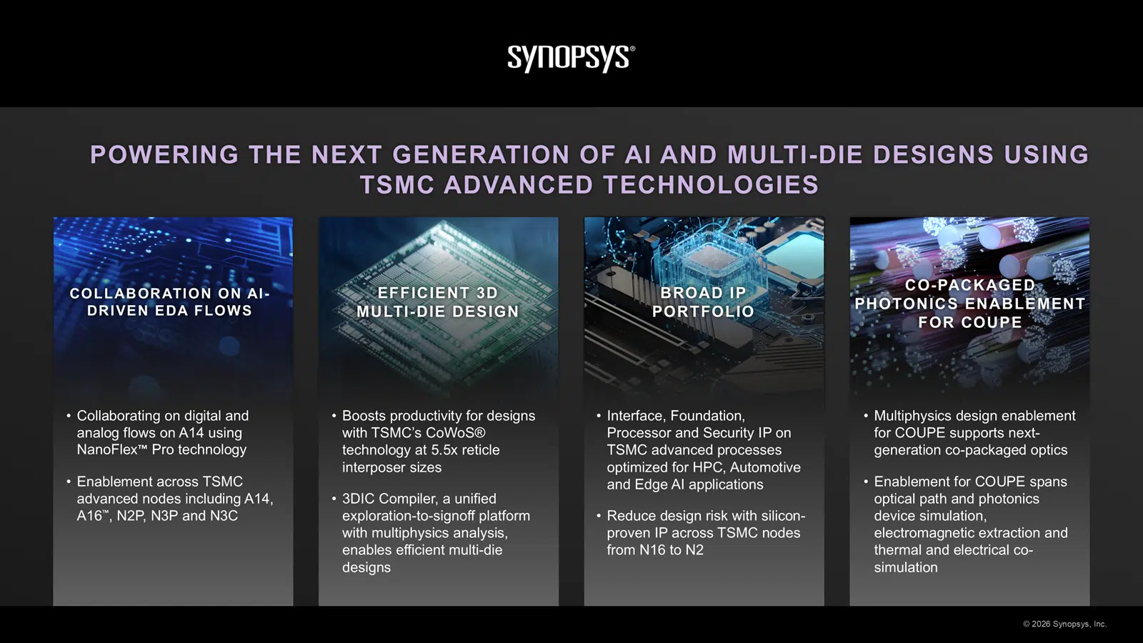
All three leading EDA vendors — Synopsys, Cadence, and Siemens EDA — issued concurrent announcements detailing their respective collaborations with TSMC. Synopsys announced silicon-proven IP advances, AI-powered EDA flows, and system-level enablement across TSMC’s N3, N2, A16, and A14 nodes, including the industry’s first low-power M-PHY v6.0 IP silicon bring-up on TSMC N2P and multiphysics design enablement for TSMC-COUPE co-packaged optics. Cadence announced an expanded partnership enabling AI design flows supporting TSMC N3, N2, A16, and A14 process nodes under its “Design for AI and AI for Design” framework. Siemens EDA announced continued collaboration with TSMC to advance AI-powered semiconductor design, building on its recently launched Fuse EDA AI Agent for autonomous multi-agent workflow orchestration and its February 2026 acquisition of Canopus AI for AI-based manufacturing metrology.
EDA Vendors Race to Align With TSMC’s Sub-2nm AI Roadmap
Analyst Take: As process and packaging complexity escalates, the design tool ecosystem has become as strategically consequential as the silicon itself. Each vendor is staking out a differentiated position — Synopsys leading on silicon-proven IP depth and multiphysics signoff uniquely suited to photonics, Cadence on breadth of node coverage and an AI-native platform vision, and Siemens EDA on agentic AI orchestration and design-to-manufacturing integration. The divergence in strategies reflects the reality that no single EDA approach can address the full spectrum of challenges posed by TSMC’s expanding portfolio of sub-2nm nodes, advanced packaging, co-packaged optics, and automotive-grade processes. With TSMC concentrating an unprecedented number of production milestones in the 2028-2029 window, the EDA vendors that can deliver certified, production-ready flows fastest will disproportionately capture the design starts that lock in long-term customer relationships.
Synopsys’ Multiphysics Stack Makes It the Natural COUPE Design Partner
Synopsys’ announcement centers on concrete silicon milestones rather than architectural vision, but it is the TSMC-COUPE enablement that most clearly differentiates its position among the three vendors. The successful tape-out of 224G IP for co-packaged optical Ethernet and UALink on TSMC-COUPE, combined with 3D IC enablement for TSMC-SoIC on A14, demonstrates that Synopsys has production-ready IP at the precise intersection where electrical and optical domains converge on a single package. TSMC-COUPE’s 2x power efficiency and 10x latency reduction versus pluggable alternatives come with a design verification burden that demands co-simulation across thermal, electrical, optical, and electromagnetic physics — a capability that Synopsys’ post-Ansys acquisition tool stack, spanning RedHawk-SC for digital power integrity, Totem-SC for analog power integrity, and Ansys-derived optical and electromagnetic solvers, is uniquely positioned to deliver.
Futurum Research has identified co-packaged optics as poised for meaningful adoption in AI networking by the end of the decade, making the EDA vendor that solves multiphysics signoff for these architectures an early and durable winner. The agentic run assistance in Fusion Compiler on TSMC A14 using NanoFlex Pro architecture and the 5.5x reticle CoWoS productivity improvements in 3DIC Compiler address the most immediate packaging bottleneck facing AI accelerator designers today. Synopsys’ Ansys-derived multiphysics portfolio transforms from a strategic acquisition rationale into a concrete competitive moat precisely because TSMC-COUPE creates a design problem that no other EDA vendor’s current tool stack can fully address.
Cadence Bets on Platform Breadth and AI-Native Architecture as the Wedge
Cadence’s announcement emphasizes coverage across four generations of TSMC process nodes — N3, N2, A16, and A14 — representing the broadest explicit node span among the three vendors’ announcements. The “Design for AI and AI for Design” framework articulates a dual strategy: optimizing tools for the specific demands of AI chip architectures while simultaneously applying AI and machine learning (ML) to accelerate every phase of the chip design process, from register-transfer level (RTL) through back-end physical design. Cadence CEO Anirudh Devgan’s remarks at CadenceLIVE 2026, delivered days before the TSMC Symposium, framed the JedAI platform with GPU acceleration as the unifying environment for this vision, with core engine improvements cited at 7% better-placed area on 2nm designs and 2X to 2.5X improvement in logic simulation through chiplet-optimized partitioning.
The emphasis on hyperscaler customers reflects a pragmatic recognition that the largest AI chip design budgets and the most complex tape-outs are concentrated among a small number of cloud and AI infrastructure providers building on TSMC’s most advanced nodes. Cadence’s explicit callout of physical AI and three-dimensional integrated circuit (3D IC) design as growth vectors aligns directly with TSMC’s expanding 3DFabric portfolio, though its announcement provides fewer specific COUPE-related milestones than Synopsys, leaving a question about how quickly Cadence can close the multiphysics gap that co-packaged optics demand. The takeaway is that Cadence is betting that platform breadth and an AI-native architecture will prove more durable than any single IP proof point, but the emergence of TSMC-COUPE as a production technology in 2026 creates a near-term opening that favors vendors with cross-domain simulation capabilities already in hand.
Siemens EDA Pursues a Flanking Strategy Through Agentic Autonomy
Siemens EDA’s TSMC collaboration announcement arrives in a fundamentally different competitive context than those of Synopsys and Cadence, reflecting the company’s smaller foundry-facing footprint but more aggressive AI architectural ambitions. The Fuse EDA AI Agent, launched in March 2026, represents a distinct approach: rather than embedding AI within individual tools, Siemens is building an autonomous orchestration layer that coordinates multi-agent workflows across its complete EDA portfolio from design conception through manufacturing. The February 2026 acquisition of Canopus AI extends this strategy into AI-based semiconductor manufacturing metrology, giving Siemens a design-to-fabrication AI narrative that neither Synopsys nor Cadence has fully articulated.
Siemens’ keynote claim at SEMICON China 2026 that agentic AI could cut entire chip design cycles in half is the boldest efficiency assertion among the three vendors, though it remains to be validated at production scale on TSMC’s most advanced nodes. The collaboration with TSMC on 3D IC and advanced packaging enablement represents a focused niche play that leverages Siemens’ parent company strength in industrial simulation and digital twin technology. Siemens EDA may be conceding IP portfolio depth to Synopsys and node coverage breadth to Cadence while attempting to leapfrog both on the AI orchestration layer that governs how design tools are used.
TSMC’s 2029 Convergence with Optics Tests EDA’s Scaling Limits
TSMC’s roadmap concentrates on A13, A12, beyond-14-reticle CoWoS, System-on-Wafer eXtreme (SoW-X), and advanced SoIC milestones in the 2029 production window, creating a simultaneous multi-technology ramp that will stress the EDA ecosystem as much as it does the foundry itself. Each new process variant and packaging configuration requires dedicated design rule decks, certified signoff flows, characterized IP blocks, and validated reference methodologies — and the three EDA vendors must deliver these in parallel across overlapping timelines. The competitive dynamics are intensified by the fact that design starts on A14, and A16 is underway now, meaning the EDA flows certified today will determine which vendors capture the downstream migration to A13 and A12 when those nodes reach production.
The production entry of TSMC-COUPE in 2026 introduces a design verification challenge that is qualitatively different from anything the EDA ecosystem has previously confronted at scale, because co-packaged optics require the simultaneous optimization of photonic waveguides, electrical interconnects, thermal dissipation, and electromagnetic interference on a shared substrate. Futurum Research’s report on Co-Packaged Optics has identified that AI workloads are driving exponential bandwidth demand that outpaces current pluggable optics capabilities, making co-packaged optics essential for future AI infrastructure scaling, but the design tool implications of this transition have received far less attention than the networking benefits.
TSMC’s announcement that COUPE delivers 2x power efficiency and 10x latency reduction versus pluggable alternatives validates the performance case, yet these gains come with signoff complexity that demands tools capable of reasoning across physical domains that have historically been addressed by separate tool chains owned by separate engineering teams. Among the three EDA vendors, only Synopsys has announced specific COUPE design enablement — 224G IP for co-packaged optical Ethernet and UALink — while Cadence and Siemens have not yet disclosed comparable COUPE-specific milestones. COUPE enters production in 2026, meaning the design for next-generation co-packaged optics architectures is underway now, and the EDA vendor with certified flows and proven IP will capture those tape-outs before competitors can close the gap.
What to Watch:
- Whether Synopsys’ multiphysics signoff advantage from the Ansys acquisition translates into measurable COUPE design-win gains before Cadence or Siemens can field comparable cross-domain tools
- How Cadence’s JedAI platform and GPU acceleration perform at production scale on TSMC A14 and A16 tape-outs, and whether the platform can be extended to address co-packaged optics signoff
- Whether Siemens EDA’s Fuse AI Agent can demonstrate autonomous design optimization on TSMC’s most advanced nodes
- How automotive EDA demand evolves as TSMC’s N2A approaches AEC-Q100 qualification, creating a new design complexity vector that spans functional safety and nanosheet physics
- Whether the co-packaged optics design challenge accelerates EDA industry consolidation or creates space for specialist photonic design tool vendors to emerge alongside the established three
See the complete press release on TSMC’s advanced process technology on Business Wire.
Disclosure: Futurum is a research and advisory firm that engages or has engaged in research, analysis, and advisory services with many technology companies, including those mentioned in this article. The author does not hold any equity positions with any company mentioned in this article.
Analysis and opinions expressed herein are specific to the analyst individually and data and other information that might have been provided for validation, not those of Futurum as a whole.
Other Insights from Futurum:
CadenceLIVE 2026 — Can Agentic AI Finally Crack 3D IC Design Automation?
Synopsys Converge – Is the New Synopsys Ready to Own Multi-Physics Design?
Can Cadence Shorten Chip Design Timelines with ChipStack AI?
Author Information

Brendan is Research Director, Semiconductors, Supply Chain, and Emerging Tech. He advises clients on strategic initiatives and leads the Futurum Semiconductors Practice. He is an experienced tech industry analyst who has guided tech leaders in identifying market opportunities spanning edge processors, generative AI applications, and hyperscale data centers.
Before joining Futurum, Brendan consulted with global AI leaders and served as a Senior Analyst in Emerging Technology Research at PitchBook. At PitchBook, he developed market intelligence tools for AI, highlighted by one of the industry’s most comprehensive AI semiconductor market landscapes encompassing both public and private companies. He has advised Fortune 100 tech giants, growth-stage innovators, global investors, and leading market research firms. Before PitchBook, he led research teams in tech investment banking and market research.
Brendan is based in Seattle, Washington. He has a Bachelor of Arts Degree from Amherst College.