Analyst(s): Brendan Burke
Publication Date: April 10, 2026
Intel has confirmed a manufacturing partnership with Tesla, SpaceX, and xAI under the Terafab project, committing its 18A process node and advanced packaging capabilities to a consolidated fabrication campus in Texas. The agreement represents the most significant external foundry contract in Intel’s history, with implications for U.S. semiconductor supply chain structure and the competitive dynamics of the global foundry market.
What is Covered in This Article:
- Intel’s Terafab partnership with Tesla, SpaceX, and xAI
- Advanced packaging as a domestic alternative to constrained supply
- Consolidated fabrication and supply chain deglobalization
- Memory and equipment procurement as scaling constraints
The News: Intel confirmed a manufacturing partnership with Tesla, SpaceX, and xAI under the name Terafab, a project to build a semiconductor fabrication campus at the Giga Texas site in Austin, Texas. The facility is designed to colocate design, lithography, fabrication, memory integration, and advanced packaging within a single 100-million-square-foot campus, with a stated target of producing one terawatt of computing power annually.
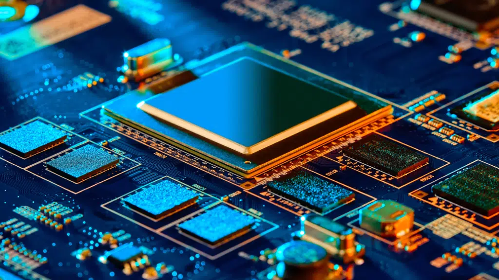
Intel’s contribution centers on its 18A process node, which incorporates gate-all-around (GAA) transistor architecture and backside power delivery, along with its embedded multi-die interconnect bridge (EMIB) and Foveros 3D stacking packaging technologies. Approximately 20% of the planned capacity is allocated to edge inference processors for Tesla’s autonomous driving systems, the Cybercab fleet, and the Optimus humanoid robot program, while the remaining 80% is designated for the D3 radiation-hardened chip intended for SpaceX satellite constellations.
Intel CEO Lip-Bu Tan characterized the effort as a “step change in how silicon logic, memory, and packaging will get built in the future.”
Can Intel Foundry’s Advanced Packaging Bring the Terafab Vision to the Stars?
Analyst Take: The Intel Terafab partnership reshapes the competitive calculus for Intel Foundry by delivering the kind of high-profile anchor customer commitment the company has struggled to secure since launching its external foundry strategy. Pairing Intel’s 18A process and advanced packaging portfolio with Tesla, SpaceX, and xAI as dedicated customers moves the foundry business from aspiration to execution in a single announcement. The consolidated campus model, which collapses a globally distributed fabrication workflow into a single domestic site, represents the most aggressive attempt at semiconductor supply chain regionalization to date. The central tension is whether the technical foundation and capital structure can support ambitions that span edge inference, orbital computing, and advanced memory integration at the scale described. The Intel Terafab foundry partnership will be measured not by the boldness of the vision but by yield curves, equipment procurement timelines, and the durability of its customer commitments.
The Foundry Credibility Gap Narrows
Intel Foundry’s most persistent challenge under CEO Lip-Bu Tan has been persuading external customers that its manufacturing capabilities merit long-term volume commitments. The company’s 18A process node, now in volume manufacturing with yield stabilization reported near 65% at its Arizona facilities, provides a technical basis for external engagement, but process readiness alone has not been sufficient to close the trust deficit. Securing Tesla, SpaceX, and xAI as anchor customers changes the optics substantially, because these are among the most demanding silicon consumers in the market, spanning autonomous vehicles, humanoid robotics, and frontier AI workloads.
The partnership also provides Intel with predictable wafer demand to improve capacity utilization economics, a factor that has weighed on the foundry’s financial profile. Beyond volume, the arrangement functions as a technology validation exercise, requiring Intel to demonstrate that its full stack of process, packaging, and design enablement capabilities can serve customers whose requirements rival those of hyperscale cloud providers. The implication is that Terafab converts Intel Foundry from a theoretical alternative to an operational one with named, high-volume customers attached.
Advanced Packaging as the Strategic Differentiator
The packaging dimension of Terafab may carry more competitive weight than the process node itself, given the structural constraints in the global advanced packaging market. TSMC’s chip-on-wafer-on-substrate (CoWoS) platform remains the standard for high-density AI accelerator packaging, and its capacity is fully allocated through at least 2028, leaving customers with limited alternatives for heterogeneous integration at scale. Intel’s EMIB and Foveros technologies, particularly the newer EMIB-T variant designed for future high-bandwidth memory needs, offer a domestic second-source pathway for customers who cannot secure CoWoS capacity.
The Terafab campus model amplifies this advantage by placing packaging operations adjacent to fabrication, eliminating the logistical latency of shipping wafers between geographically dispersed facilities. Intel’s recent research into gallium nitride (GaN) power chiplets, including a 19-micrometer-thick GaN-on-silicon chiplet with integrated complementary metal-oxide-semiconductor (CMOS) control circuits, introduces the possibility of heterogeneous power delivery within the same advanced package. Intel’s packaging portfolio, rather than its process node alone, may prove to be the most defensible competitive asset that Terafab brings to the foundry market.
A Consolidated Campus Challenges the Distributed Model
The prevailing semiconductor supply chain model distributes fabrication, memory integration, and packaging across multiple countries, with wafers typically fabricated in Taiwan, memory integrated in South Korea, and packaging in Southeast Asia. Terafab proposes to collapse this chain into a single campus where engineers can test and revise lithography masks within the same facility, reducing the weeks-long cycle times inherent in international logistics. This colocation model offers structural advantages in iteration speed and intellectual property containment, both of which matter to customers operating in defense-adjacent and autonomous systems markets.
The U.S. government’s equity position in Intel and $11.1 billion in federal investment underscore the geopolitical alignment between this project and broader policy objectives to localize semiconductor manufacturing for aerospace and transportation infrastructure. However, consolidation also concentrates risk, as a single-site dependency across multiple chip architectures exposes it to regional disruptions such as power, water, and labor constraints. The consolidated campus model trades geographic diversification risk for logistical efficiency and speed, a tradeoff whose viability depends on the robustness of local infrastructure at scale.
Scaling Constraints Define the Execution Horizon
The stated target of one terawatt of annual compute output introduces scaling requirements that extend well beyond current industry capacity in multiple dimensions. Extreme ultraviolet (EUV) lithography tools, manufactured exclusively by ASML, are fully allocated to existing customers through 2027, meaning Terafab’s incremental equipment needs cannot be met without either displacing existing buyers or waiting for ASML’s capacity expansion. Memory fabrication presents a parallel constraint. Capital expenditure estimates ranging from $5 trillion to $13 trillion over the project’s lifespan place Terafab in a financial category without precedent, even accounting for the SpaceX-xAI merger and a planned SpaceX initial public offering targeting $50 billion to $80 billion in proceeds.
The gap between available financing mechanisms and stated capital requirements suggests that the full-scale vision will unfold over decades rather than years, with phased capacity buildouts dependent on sustained government co-investment and equipment availability. Equipment procurement, memory partnerships, and capital deployment timelines will determine whether Terafab achieves its stated scale or operates as a more modest, yet still significant, Intel Foundry expansion with dedicated anchor customers. Terafab’s near-term value lies in the credibility and volume it delivers to Intel Foundry today, while its full-scale ambitions remain contingent on solving constraints that no single entity currently controls.
What to Watch:
- Whether Intel secures confirmed ASML EUV allocations beyond its existing equipment commitments to support Terafab’s incremental capacity needs.
- The degree to which memory fabrication partnerships with incumbent producers such as SK Hynix, Micron, or Samsung emerge to address the facility’s DRAM requirements.
- Whether the SpaceX initial public offering proceeds and structure provide sufficient capital to fund early-phase construction and equipment procurement.
- How Intel’s 18A yield trajectory evolves beyond the reported 65% stabilization, and whether yield improvements translate into cost-competitive volume production for external customers.
See the full post on Intel’s Terafab partnership announcement on the Intel X account.
Disclosure: Futurum is a research and advisory firm that engages or has engaged in research, analysis, and advisory services with many technology companies, including those mentioned in this article. The author does not hold any equity positions with any company mentioned in this article.
Analysis and opinions expressed herein are specific to the analyst individually and data and other information that might have been provided for validation, not those of Futurum as a whole.
Other Insights from Futurum:
Intel Bets on Agentic AI Economics with SambaNova Partnership
Is Tesla’s Multi-Foundry Strategy the Blueprint for Record AI Chip Volumes?
Image Credit: Pushkar Ranade on X
Author Information

Brendan is Research Director, Semiconductors, Supply Chain, and Emerging Tech. He advises clients on strategic initiatives and leads the Futurum Semiconductors Practice. He is an experienced tech industry analyst who has guided tech leaders in identifying market opportunities spanning edge processors, generative AI applications, and hyperscale data centers.
Before joining Futurum, Brendan consulted with global AI leaders and served as a Senior Analyst in Emerging Technology Research at PitchBook. At PitchBook, he developed market intelligence tools for AI, highlighted by one of the industry’s most comprehensive AI semiconductor market landscapes encompassing both public and private companies. He has advised Fortune 100 tech giants, growth-stage innovators, global investors, and leading market research firms. Before PitchBook, he led research teams in tech investment banking and market research.
Brendan is based in Seattle, Washington. He has a Bachelor of Arts Degree from Amherst College.