Analyst(s): Brendan Burke
Publication Date: April 24, 2026
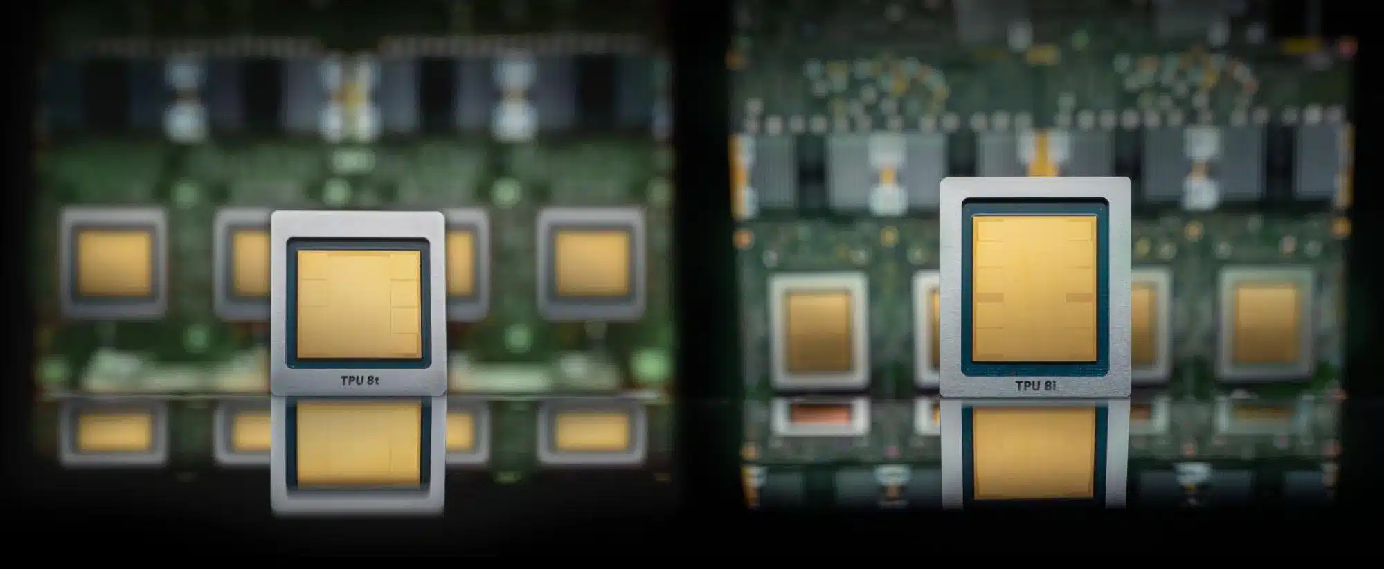
Google has unveiled its eighth-generation Tensor Processing Units (TPUs) as two separate chips, the TPU 8t for training and the TPU 8i for inference, representing a fundamental shift in how the company designs custom AI silicon. The dual-chip strategy signals that workload specialization in AI accelerators has reached a tipping point, with implications for competitive positioning across the hyperscaler landscape and for enterprise buyers evaluating cloud AI infrastructure.
What is Covered in This Article:
- Google’s eighth-generation TPU split into training and inference chips
- Workload specialization as a structural shift in AI accelerator design
- The role of network co-design in optimizing inference latency
- Goodput as an emerging metric for real-world training efficiency
- Google’s concurrent NVIDIA Vera Rubin availability on Google Cloud
The News: Google announced TPU 8t and TPU 8i at Google Cloud Next on April 22, 2026, marking the first time the company has split its TPU line into two distinct chips optimized for separate workloads:
- TPU 8t is designed for large-scale training, delivering 121 exaflops per superpod with 9,600 chips, over 2 petabytes (PB) of shared High Bandwidth Memory (HBM), native FP4 support in its Matrix Multiply Units (MXUs), and Axion Arm-based host processors.
- TPU 8i targets inference and reinforcement learning, tripling on-chip SRAM to 384 megabytes (MB), increasing HBM by 50% to 288 gigabytes (GB), and introducing a new Collectives Acceleration Engine.
Alongside the TPU announcements, Google confirmed that Google Cloud will be among the first to offer NVIDIA’s upcoming Vera Rubin system, paired with Google’s new Virgo network for large-scale training clusters.
Amin Vahdat, Vice President and General Manager of ML, Systems, and Cloud AI at Google, stated that the eighth-generation TPUs are “two chips for the agentic era,” reflecting the company’s view that training and inference workloads now require fundamentally different hardware architectures.
Google Splits Its TPU Line to Enter the Era of Agentic Silicon
Analyst Take: Google’s decision to bifurcate its TPU line into dedicated training and inference chips marks a structural evolution in how hyperscalers approach custom AI silicon, and it aligns with the broader industry shift toward systemic co-design identified in the Futurum Signal Report on AI Accelerators. The dual-chip strategy acknowledges that the computational profiles for frontier model training and low-latency Google TPU AI accelerator inference have diverged to the point where a single architecture can no longer optimally serve both.
This move places Google alongside AWS and NVIDIA, which have pursued similar disaggregation with their Trainium and Rubin inference architecture via Cerebras and Groq integrations, respectively, for agentic inference. The key tension is whether workload specialization at this level delivers a durable competitive advantage or simply raises the silicon engineering burden without proportional returns. Software complexity already weighs on the TPU’s Ecosystem Alignment score in the Futurum Signal on AI Accelerators, and this additional complexity may make the system even less operable outside of close engagements with the top AI labs.
Network Co-Design as the Defining Inference Architecture Choice
The TPU 8i’s most strategically significant feature may not be its tripled SRAM or expanded HBM, but rather the network topology surrounding it. Google’s Boardfly topology was co-designed with DeepMind to optimize for latency rather than bandwidth. Rather than arranging chips in a conventional mesh or torus, where data hops through intermediate nodes, Boardfly is engineered to minimize the number of hops between any two chips in an inference cluster, trading some aggregate bandwidth for dramatically lower point-to-point latency. The co-design with DeepMind is significant, as the topology was shaped by real agentic workload profiles rather than theoretical benchmarks, tuning the fabric specifically for the kinds of short, sequential model calls that characterize agent-based systems.
This reflects a deliberate architectural bet on the agentic AI paradigm, where minimum time-to-response defines the customer experience. It stands in contrast to training-oriented network designs that prioritize aggregate bandwidth for gradient synchronization across thousands of chips. For inference workloads that chain multiple model calls in sequence, such as those found in agent-based systems, network latency compounds at each step and becomes the binding constraint on end-to-end performance.
The introduction of the Collectives Acceleration Engine addresses this directly. In distributed inference, collective operations such as all-reduce, all-gather, and broadcast are the routines that synchronize data and activations across chips between model layers. Traditionally, these run on the same compute cores handling matrix multiplication, creating contention and idle time. Our Q2 2026 State of the Market Report (link for Futurum Intelligence subscribers) cited Matrix Core Underutilization as one of the five bottlenecks of agentic silicon. The Collectives Acceleration Engine resolves this bottleneck by offloading these communication routines entirely, allowing the main TPU compute cores to stay saturated on tensor math while synchronization happens in parallel on a separate execution path. The net effect is a reduction in the latency valleys that appear at layer boundaries in large distributed models.
Goodput Over Peak FLOPs as the Real Measure of Scale
An underappreciated dimension of Google’s announcement is its emphasis on goodput, the fraction of theoretical compute that translates into useful training throughput, rather than headline FLOPs. At a 10,000-chip scale, fail-stop failures and silent data corruption quietly erode training productivity, and Google claims more than 97% goodput at that scale. This metric matters because the gap between peak performance and realized performance widens as clusters grow, making raw FLOPs an increasingly misleading indicator of actual capability.
The Futurum Signal on AI Accelerators notes that competitive differentiation now stems from systemic co-design of data movement across billions of transistors, and goodput is the metric that captures whether that co-design actually works under production conditions. Enterprises evaluating AI infrastructure should increasingly scrutinize goodput claims rather than accepting peak FLOPs as a proxy for training efficiency.
The Multi-SKU Cadence Signals an Accelerated Silicon Roadmap
Google hinted that producing more than two TPU SKUs per year is plausible going forward, signaling an acceleration of its custom silicon roadmap that mirrors the rapid generational cadence seen across the AI accelerator market. For Google, the ability to sustain a multi-SKU annual cadence depends on maintaining the tight co-design loop between DeepMind’s model architecture research and the TPU hardware engineering team. The TPU 8t’s native FP4 support in MXUs and Axion Arm host integration suggests that each generation is being tailored to specific model training techniques rather than offering generic compute improvements. This approach carries execution risk, as dual-chip development and annual cadence acceleration double the engineering surface area. Google is committing to a silicon roadmap velocity that will test its organizational capacity but could yield compounding advantages if sustained.
NVIDIA Vera Rubin on Google Cloud Redefines Coopetition
Google’s simultaneous announcement of its own eighth-generation TPUs and its commitment to offer NVIDIA’s Vera Rubin GPU on Google Cloud sends a clear coopetitive signal to enterprise buyers. The decision to pair Vera Rubin with Google’s own Virgo network for the largest training clusters positions Google Cloud as an infrastructure-agnostic platform rather than a captive TPU environment. This is strategically significant because it directly addresses the primary friction point for enterprises whose AI stacks are built on NVIDIA’s CUDA ecosystem, allowing them to remain on Google Cloud without abandoning their existing software investments. For NVIDIA, the arrangement validates that even hyperscalers with mature custom silicon programs still see value in offering its GPUs, reinforcing the durability of NVIDIA’s ecosystem position. The takeaway is that Google’s dual-silicon strategy, offering both its own TPUs and NVIDIA’s GPUs, transforms the competitive dynamic from a zero-sum chip war into a platform-level competition for AI workload share.
What to Watch:
- Whether Google delivers concrete goodput benchmarks for TPU 8t at the claimed 97% level once production clusters are deployed at scale.
- How quickly the TPU 8i’s latency-optimized Boardfly network topology translates into measurable cost-per-token advantages for inference customers.
- ASIC designers selected for successive TPU generations
- How enterprise customers allocate workloads between Google’s TPUs and NVIDIA Vera Rubin GPUs on Google Cloud, and whether this shifts cloud provider selection dynamics.
- Whether AWS accelerates its own Trainium4 timeline or introduces further workload-specific silicon variants in response to Google’s dual-chip approach.
See the full press release on Google’s TPU 8t and TPU 8i announcement on the company website.
Disclosure: Futurum is a research and advisory firm that engages or has engaged in research, analysis, and advisory services with many technology companies, including those mentioned in this article. The author does not hold any equity positions with any company mentioned in this article.
Analysis and opinions expressed herein are specific to the analyst individually and data and other information that might have been provided for validation, not those of Futurum as a whole.
Other Insights from Futurum:
AI Accelerators – Futurum Signal
Anthropic’s Gigawatt-Scale TPU Deal with Broadcom Creates a Structural Advantage
Google Debuts Ironwood TPU to Drive Inference-Focused AI Architecture at Scale
Author Information

Brendan is Research Director, Semiconductors, Supply Chain, and Emerging Tech. He advises clients on strategic initiatives and leads the Futurum Semiconductors Practice. He is an experienced tech industry analyst who has guided tech leaders in identifying market opportunities spanning edge processors, generative AI applications, and hyperscale data centers.
Before joining Futurum, Brendan consulted with global AI leaders and served as a Senior Analyst in Emerging Technology Research at PitchBook. At PitchBook, he developed market intelligence tools for AI, highlighted by one of the industry’s most comprehensive AI semiconductor market landscapes encompassing both public and private companies. He has advised Fortune 100 tech giants, growth-stage innovators, global investors, and leading market research firms. Before PitchBook, he led research teams in tech investment banking and market research.
Brendan is based in Seattle, Washington. He has a Bachelor of Arts Degree from Amherst College.