“As Moore’s Law has slowed down, leading chipmakers are aiming to leverage various types of advanced packaging technology to improve the overall performance of semiconductor further, making advanced packaging an increasingly vital front of technology.”
Ray Wang
Research Director, Semiconductors, Supply Chain, & Emerging Tech
Advanced Packaging and HBM Capacity Remain Key Bottleneck for Global Compute
In 2H 2025, advanced packaging (AP) and HBM capacity are expected to remain critical bottlenecks for global compute deployment, driven by accelerating AI inference workloads and the growing adoption of evolving LLMs with multimodal capabilities. The technology advancement of AP and HBM and their adoption should be closely watched, as the two will underpin the future development of semiconductors used in AI servers and smartphones.
Why This Is Trending:
Memory Is Bedrock for AI Accelerator: Memory bandwidth is vital as model training is often bandwidth-constrained rather than purely compute-constrained. The attention mechanism in the transformer model has to store and calculate the relationship between all the tokens. Memory requirement is quadratic in proportion to the sequence length. Similarly, memory is also a bigger constraint during inference, due to the need to handle longer context windows and an enlarged key‑value cache (KV cache) in the transformer model. Memory consumption for KV cache grows linearly with the token size. To that end, HBM has become the essential component for AI, offering a higher speed of transferring data and lower power consumption than traditional DRAM products.
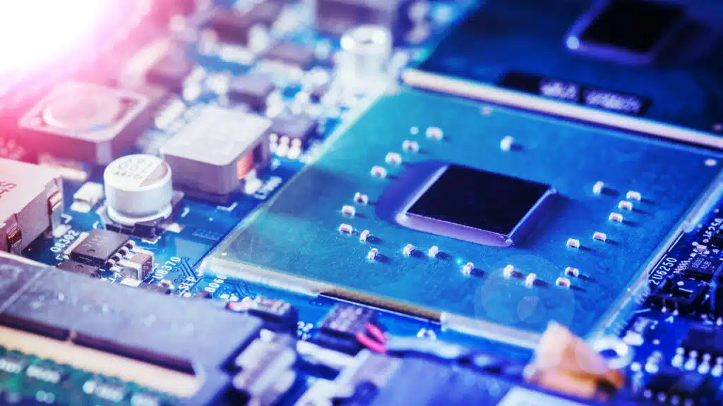
Advanced Packaging Pushes Beyond Moore’s Law: Advanced packaging has become an essential technology in the AI hardware supply chain, especially as Moore’s Law has slowed down in recent years. Chipmakers are turning to advanced packaging as a new solution to sustain performance improvements. By integrating the compute die, memory, and packaging substrate more closely, advanced packaging enables better power efficiency, higher performance, and faster data transfer between components. This is an ongoing industry shift and a key trend to follow.
Supply Constraint Remains in AI Compute: Compute demand has surged since the introduction of ChatGPT-3 in late 2022, and the acceleration of AI inference workloads has driven a second wave of growth. Today, we assess that the global compute landscape remains supply-constrained, driven not only by extraordinary demand for AI chips globally but also by structural bottlenecks across the supply chain. These include the complexity and capacity constraints of advanced packaging and HBM, technical difficulties, and slower ramp-up production in downstream assembly and integration. While compute supply–demand dynamics might be alleviated as time passes, we believe the possibility of supply constraints in compute deployment will continue in 2H 2025.
Use Cases:
HBM for GPUs and ASICs: HBM remains the critical memory technology powering nearly every major AI accelerator globally, from NVIDIA’s GB200 to Google’s TPUv6p. The fifth-generation HBM3E 12-hi is expected to be the dominant product through the remainder of 2025 and into 1H 2026. Looking ahead, SK Hynix will likely first introduce HBM4 (6th gen HBM) in the market, powering the next generation of AI chips, including NVIDIA’s VR200 and AMD’s MI400X.
Advanced Packaging (AP): Advanced packaging technologies are indispensable for all the AI chips, just like HBM. Advanced packaging for AI accelerators, such as TSMC’s CoWoS-S, CoWoS-R, and CoWoS-L, plays a critical role in not only packaging the compute die, HBM, I/O die, and other necessary components into a single AI chip but also further improving the performance of an AI accelerator. Demand for CoWoS-L has increased due to NVIDIA’s transition from Hopper GPUs to Blackwell, which is later supported by CoWoS-L technology instead of CoWoS-S. Another packaging technology to watch is WMCM (Wafer-Level Multi-Chip Module), expected to power Apple’s next-generation A20 SoC for the iPhone 18, which will come into play in 2026.
Co-Packaged Optics (CPO): CPO represents an advanced form of heterogeneous integration that combines optical components and semiconductor devices within a single package, aiming to overcome high-bandwidth data center applications’ performance and power limitations. While the industry continues to debate the commercial viability and timing of CPO adoption, the growing need for high-speed, low-power interconnect solutions makes its eventual deployment increasingly necessary. The earliest realistic timeline for CPO to enter the market is around late 2026 and 2027. One potential real-world application of CPO could be NVIDIA’s Rubin-series GPUs, which are expected in 2026, and the following Feynman product line.
About Ray:
Ray is Research Director for Semiconductors, Supply Chain, & Emerging Tech, where he will conduct analysis and advisory work for the semiconductor and AI industry. He holds an M.S. in Foreign Service from Georgetown University, where he focused on global business and technology. He previously held research and advisory roles at DGA Group, CSIS, and ITIF, focusing on semiconductors, emerging technologies, and macroeconomic policy. His works and comments have appeared on CNBC, South China Morning Post, Wall Street Journal, Fast Company, CNN, and other leading global media outlets.
Ray Wang, Research Director for Semiconductors, Supply Chain, and Emerging Technology, shares insights on Futurum’s new Silicon Tracker dataset, aiming to help industry leaders understand the AI hardware supply chain....
Ray Wang, Research Director for Semiconductors, Supply Chain, and Emerging Technology at Futurum, shares the key findings and insights from the newly launched 2H 2025 Data Center Semiconductor Decision Maker...
Ray Wang, Research Director for Semiconductors, Supply Chain, and Emerging Technology at Futurum, shares his insights and observations during the OCP Global Summit 2025, focusing on AI infrastructure....
Ray Wang, Research Director at Futurum, shares his insights on Lattice MachXO5-NX TDQ, the first CNSA 2.0-compliant PQC-ready secure control FPGA, highlighting its crypto-agility, Root of Trust, and quantum-resistant security...
Ray Wang and Daniel Newman at Futurum share their insights on how QumulusAI USD.AI financing uses tokenized GPU collateral and stablecoin liquidity to fund up to 70% of deployments, enabling...
Ray Wang, Research Director at Futurum, shares his insights on the AMD OpenAI partnership spanning 6 GW of Instinct GPUs, where milestone-linked warrants and power readiness define the next phase...
Get important insights straight to your inbox, receive first looks at eBooks, exclusive event invitations, custom content, and more. We promise not to spam you or sell your name to anyone. You can always unsubscribe at any time.
Thank you, we received your request, a member of our team will be in contact with you.