Analyst(s): Brendan Burke
Publication Date: February 11, 2026
Applied Materials launches new systems for 2nm chip production, including the Viva radical treatment for atomically smooth transistor channels, Sym3 Z Magnum for precise high-aspect-ratio etch, and Spectral ALD for low-resistance molybdenum contacts. The company claims these innovations collectively address the limitations of GAA (Gate-All-Around) architectures, which are now being adopted by multiple leading foundries to enable the energy-efficient performance needed for next-generation AI workloads.
What is Covered in this Article:
- Applied Materials’ launch of Viva radical treatment, Sym3 Z Magnum etch, and Spectral ALD systems
- The logic industry’s transition from FinFET to GAA nanosheet transistors at the 2nm node
- Engineering advances in nanosheet channel smoothing and angstrom-level process control
- The shift from tungsten to molybdenum for low-resistance, reliable contacts
- The roadmap for denser DRAM and the interplay between logic, memory, and AI compute
The News: At SEMICON Korea, Applied Materials announced a new suite of semiconductor manufacturing systems for 2nm and angstrom-class nodes, specifically engineered for Gate-All-Around (GAA) nanosheet transistors and advanced back-end interconnects. The Applied Producer Viva system performs ultra-pure radical channel treatments to reduce atomic-scale surface roughness and maximize electron mobility. The Sym3 Z Magnum etch platform uses pulsed voltage technology to create precise, vertical, high-aspect-ratio trenches, supporting both logic and 3D DRAM scaling. The Spectral ALD tool enables the industry’s shift from tungsten to molybdenum contacts, reducing electrical resistance and supporting the demands of fast-switching, energy-efficient AI chips. According to the company, these systems are now being used by multiple leading logic foundries as GAA devices ramp to volume.
Will Applied Materials’ Transistor Breakthroughs Empower 2nm AI Chips?
Analyst Take: The transition to Gate-All-Around (GAA) nanosheet transistors at the 2nm process node marks one of the semiconductor industry’s most consequential inflections since the adoption of FinFETs. GAA is the next evolution of the transistor, designed to address electrical current leakage in previous generations. Leading global foundries have begun volume production in recent months, but continue to struggle with yields.
While GAA is already celebrated for its theoretical gains of up to 20% improved logic density and up to 30% lower power consumption, its economic viability for mass production has historically been less certain. The cost-effectiveness of GAA hinges not only on device architecture but also on materials and process-control innovations that can translate design benefits into high-yield manufacturing.
Material Engineering as a Cost Lever
A central challenge in GAA production is engineering the physical and electrical properties of the nanosheet channels with atomic-scale precision. Channel surface roughness can dramatically impact yield. To enhance cutting-edge nanosheets, Applied Materials’ new Viva radical treatment system enables consistent, high-mobility channels across entire wafers by providing angstrom-level smoothing and defect removal.
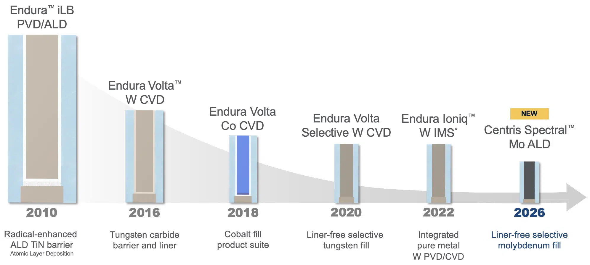
The choice of contact material is another pivotal factor in controlling device resistance and, by extension, product cost. Applied has a long history of innovation in contact materials, from tungsten carbide to cobalt to selective tungsten. In a generational leap, Applied’s Spectral ALD system introduces molybdenum (Mo) as an alternative to tungsten (W) in transistor contacts.
Molybdenum not only enables a 15% reduction in electrical resistance but also supports a more reliable bottom-up fill process, reducing the risk of performance-killing seams and voids. Lower resistance translates directly into faster switching and lower static power loss, both of which are prized for AI workloads. Reducing contact resistance in the backend is critical for power efficiency, a challenge that is directly addressed by the shift toward backside power delivery. Importantly, these benefits are realized within standard process flows, meaning fabs can upgrade throughput and device performance without absorbing the steep costs of revolutionary process overhauls.
Figure 1: Applied Materials Contact Resistance Product History
Scaling Without Sacrificing Yield
GAA’s vertical, stacked architecture demands etching capabilities that are both deep and precise. Even before GAA, the Sym3 etch system family has been the fastest scaling product in Applied Materials’ history, shipping over 13,000 chambers in 2025. The newly launched Sym3 Z Magnum etch system, featuring second-generation pulsed voltage technology, shapes high-aspect-ratio cavities with tight profile control. By minimizing sidewall variation and ensuring flat, rectangular cavity floors, fabs can achieve the consistent nanosheet lengths and contact area needed for robust performance at scale.
These process control improvements ensure that the incremental costs of moving to GAA are offset by operational efficiencies. Additionally, integrating supplemental radical treatment via innovative annealing processes further reduces copper line resistance, extending the useful life of copper as a wiring material and providing another route to cost containment.
A Path Toward Mainstream AI Silicon and Beyond
The confluence of these advancements means GAA is no longer reserved for premium-tier products where cost is secondary to absolute performance. Instead, fabs now have the tools and materials needed to bring GAA to broader classes of AI chips, data center processors, and, eventually, high-volume consumer devices. With leading foundries already adopting these systems for 2nm and ramping to volume, the supply chain implications are profound. Cost-effective GAA will not only extend continued generational gains in transistor density but will also underwrite the energy-efficient, high-throughput computing critical for sustaining the global AI race.
GAA is not just a technical marvel but now an economically viable workhorse, thanks to innovations in materials engineering, surface conditioning, and process control. As the first 2nm AI chips reach production at scale, these material and system breakthroughs may ultimately be remembered not just for enabling a new transistor, but for making next-generation silicon affordable enough to power the coming wave of AI adoption.
What to Watch:
- Adoption Velocity for 2nm GAA: Track how rapidly leading foundries and logic chip customers move Applied’s Viva, Sym3 Z Magnum, and Spectral ALD systems into high-volume manufacturing at angstrom-class nodes.
- Measurable Gains in Channel Mobility and Power: Monitor published device benchmarks and customer disclosures to validate claims of improved electron mobility, reduced resistance, and lower power consumption enabled by atomic-level surface and etch engineering.
- Integration and Yield Across Logic and Memory: Watch for evidence that radical nanosheet smoothing, vertical cavity etch, and molybdenum contacts translate into higher yield rates and cost-effective process scaling in both logic transistors and next-generation 3D DRAM.
- Impact on AI Compute Roadmaps: Assess how these materials and process innovations accelerate energy-efficient roadmap execution for AI and high-performance computing chips.
- Potential for Next-Gen Materials Expansion: Observe whether Applied’s ultra-pure plasma and molybdenum advances spur adoption of additional novel materials or new device structures beyond GAA, signaling further inflections in semiconductor manufacturing.
Read the full press release on Applied Materials’ product launch and its details on the company website.
Disclosure: Futurum is a research and advisory firm that engages or has engaged in research, analysis, and advisory services with many technology companies, including those mentioned in this article. The author does not hold any equity positions with any company mentioned in this article.
Analysis and opinions expressed herein are specific to the analyst individually and data and other information that might have been provided for validation, not those of Futurum as a whole.
Other insights from Futurum:
Applied Materials Q4 FY 2025 Results Emphasize AI-Focused Mix
Hybrid Bonding at Scale: Powering the Next Era of Semiconductor Packaging
Author Information

Brendan is Research Director, Semiconductors, Supply Chain, and Emerging Tech. He advises clients on strategic initiatives and leads the Futurum Semiconductors Practice. He is an experienced tech industry analyst who has guided tech leaders in identifying market opportunities spanning edge processors, generative AI applications, and hyperscale data centers.
Before joining Futurum, Brendan consulted with global AI leaders and served as a Senior Analyst in Emerging Technology Research at PitchBook. At PitchBook, he developed market intelligence tools for AI, highlighted by one of the industry’s most comprehensive AI semiconductor market landscapes encompassing both public and private companies. He has advised Fortune 100 tech giants, growth-stage innovators, global investors, and leading market research firms. Before PitchBook, he led research teams in tech investment banking and market research.
Brendan is based in Seattle, Washington. He has a Bachelor of Arts Degree from Amherst College.