Analyst(s): Brendan Burke
Publication Date: January 27, 2026
What is Covered in this Article:
- Why the challenge facing co-packaged optics (CPO) has shifted from optical performance to systems integration
- How cross-domain engineering lessons from aerospace, defense, and automotive are reshaping CPO workflows
- Why thermal materials, testing infrastructure, and simulation now gate AI-scale deployment
- How adjacent photonics innovations signal ecosystem maturity
The Event — Major Themes & Vendor Moves: SPIE Photonics West 2026, held at San Francisco’s Moscone Center, drew more than 20,000 attendees across light-based science and technology. The annual conference spans the full photonics stack from fundamental materials and devices to applications in data centers, telecommunications, sensing, automotive, aerospace, and defense. This year’s event presented co-packaged optics no longer framed as a future bandwidth solution, but as a near-term systems engineering challenge that demands maturity across simulation, materials, and manufacturing.
Panelists and technical talks emphasized simulation and testing capabilities to optimize optical system design. Supporting this pivot, vendors introduced enabling technologies that target the practical gates to CPO scale, including thermal density, precise spectral control, and production-grade metrology and test. With the Optical Fiber Communication Conference (OFC) upcoming in March and strengthening ties between the photonics community and hyperscalers, this show offered a chance to share foundational progress that systems can be built on.
Did SPIE Photonics West 2026 Set the Stage for Scale-up Optics?
Analyst Take: Co-packaged Optics Poised for Scale
CPO Is Now a Systems Engineering Problem
The most important signal from SPIE was the industry’s collective admission that co-packaged optics can no longer be designed in silos. A panel discussion moderated by Ellen Schelew of Ansys, part of Synopsys, with panelists from BAE Systems, Ayar Labs, and Tesla drew direct parallels between CPO and mature aerospace and automotive workflows, where multi-disciplinary constraints, strict tolerances, and ecosystem standards are non-negotiable. In hyperscale data centers, CPO designers now face the same multi-domain coupling challenges where optical, thermal, mechanical, and electrical effects are modeled concurrently from day one. This approach is beginning to prove successful with the integration of CPO in next-generation advanced accelerator packaging.
The Ansys team from Synopsys presented a technical paper showing how GPU-accelerated simulation enables the optimization of optical couplers, thermal interactions, and electrical-optical links that may previously have proven error-prone. The speed-up of engineering simulations enables exploration of CPO design spaces at AI-relevant scales. Because of the complex dependencies of AI systems, vendors that lack integrated simulation and optimization are likely to fall behind, regardless of optical IP maturity.
Thermal and Test Infrastructure Remain Deployment Gates
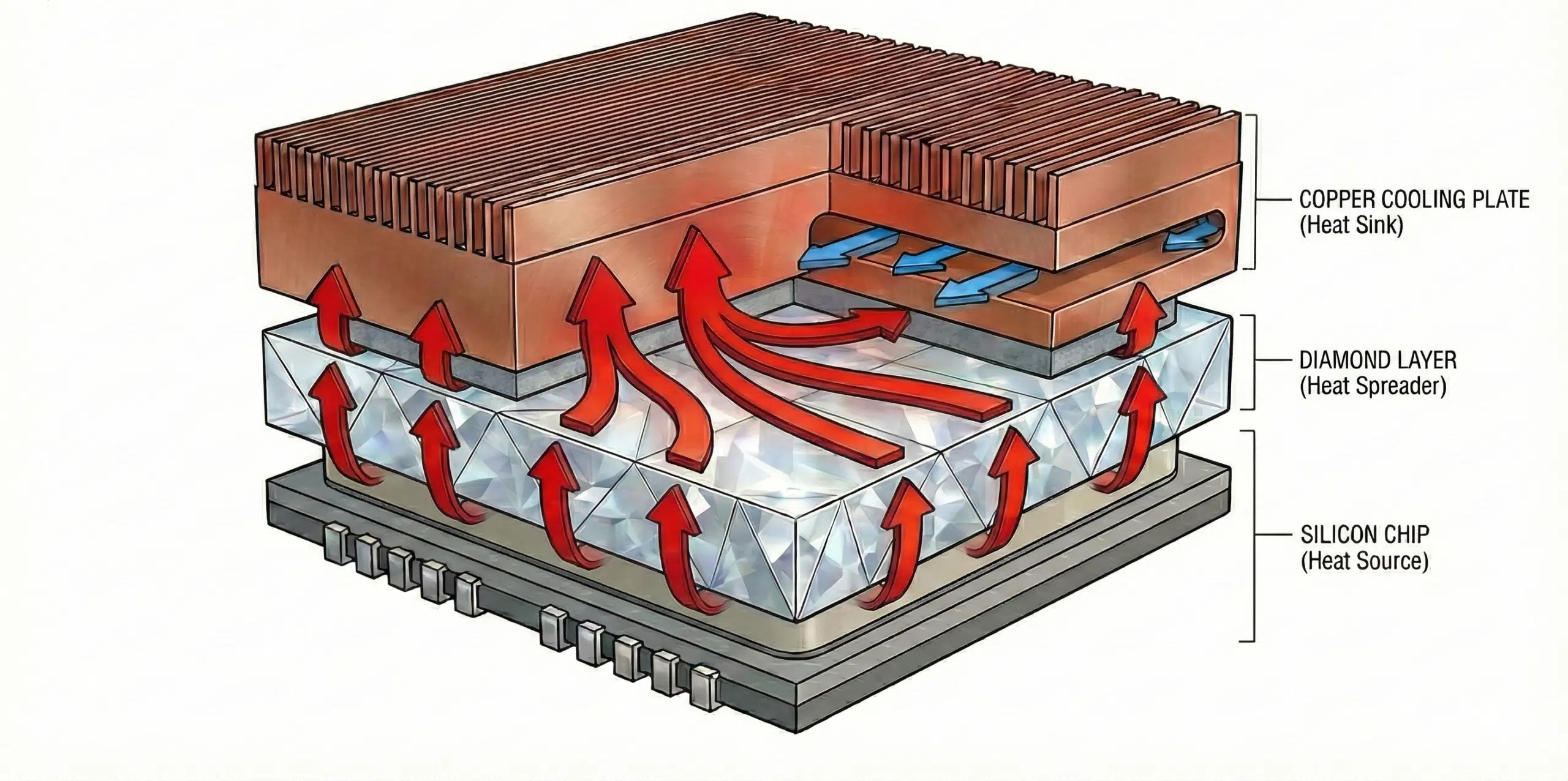
In advanced materials, Coherent launched bondable diamond thermal spreaders to address the thermal density problem. Diamond cooling addresses the most thermally stressed segment between silicon and the cooling plate. By spreading heat up to 5x more efficiently than copper and reducing localized hotspots, diamond enables higher sustained utilization without increasing power draw. As advanced packaging concentrates heat and data center power budgets harden, incremental gains at the thermal interface are one of the few remaining ways to unlock meaningful system-level efficiency. Through materials innovation, Coherent supports the coexistence of its optical products with high-power switches and accelerators. The company also showcased recent innovations, including laser power metrology that can validate optical links.
Figure 1: Indicative Direct Bonded Diamond Thermal Spreading Design
On the other side of the deployment gate is testing. You can’t scale what you can’t test at production volume. At SPIE, Quantifi Photonics introduced a PCI-based continuous wave external laser source designed to scale CPO manufacturing tests. CPO introduces orders-of-magnitude increases in channel count, power density, and integration complexity. This complexity requires instrumentation aligned with production-grade reliability. Reliability is a hurdle that must be surmounted before data center architects will make the switch from copper to optics within server racks.
Photonics Platforms Are Becoming Secure Infrastructure
Coherent’s demonstration with Quside of a mass-manufacturable quantum entropy source adds an important adjacent signal to the CPO narrative. By showing that cryptographic randomness can be generated from vertical-cavity surface-emitting laser (VCSEL) processes, which are scaling into scale-out AI interconnects, the collaboration moves quantum-grade security from niche deployments into mainstream hardware. Once photonic manufacturing can reliably deliver security primitives alongside optical performance, photonics can gain trust as the backbone of data centers in the post-quantum era.
Designing for Reliability
AI giants are showing interest in expanding their usage of photonics to build AI factories and achieve high-speed interconnects within racks. And yet, we are still looking for the supply chain and engineering stack to deliver mature solutions at scale. SPIE’s technical sessions and vendor panels highlighted that CPO demands a new level of cross-discipline integration. Success now depends on integrating optical engines with high-power ASICs, packaging with advanced materials and processes, and validating them through production-grade, high-channel-count test regimes. We expect further breakthroughs this year in both systems engineering and throughput for pluggable transceivers and CPO.
What to Watch:
- The extent to which hyperscalers operationalize multi-physics simulation and integrated design workflows for CPO development
- Progress toward standardized and interoperable CPO test methodologies across the ecosystem
- The transition of diamond and advanced photonic materials from niche solutions to industry-standard components in high-volume manufacturing
- The evolution of photonics platforms beyond high-speed connectivity to security, sensing, and broader system-level capabilities within next-generation infrastructure
You can read more at SPIE Photonics West website and participating vendors’ websites.
Disclosure: Futurum is a research and advisory firm that engages or has engaged in research, analysis, and advisory services with many technology companies, including those mentioned in this article. The author does not hold any equity positions with any company mentioned in this article.
Analysis and opinions expressed herein are specific to the analyst individually and data and other information that might have been provided for validation, not those of Futurum as a whole.
Other insights from Futurum:
AWS European Sovereign Cloud Debuts with Independent EU Infrastructure
Modern Private Cloud: Balancing Operational Agility with Data Sovereignty
At CES, NVIDIA Rubin and AMD “Helios” Made Memory the Future of AI
Author Information

Brendan is Research Director, Semiconductors, Supply Chain, and Emerging Tech. He advises clients on strategic initiatives and leads the Futurum Semiconductors Practice. He is an experienced tech industry analyst who has guided tech leaders in identifying market opportunities spanning edge processors, generative AI applications, and hyperscale data centers.
Before joining Futurum, Brendan consulted with global AI leaders and served as a Senior Analyst in Emerging Technology Research at PitchBook. At PitchBook, he developed market intelligence tools for AI, highlighted by one of the industry’s most comprehensive AI semiconductor market landscapes encompassing both public and private companies. He has advised Fortune 100 tech giants, growth-stage innovators, global investors, and leading market research firms. Before PitchBook, he led research teams in tech investment banking and market research.
Brendan is based in Seattle, Washington. He has a Bachelor of Arts Degree from Amherst College.